|
|
|
|
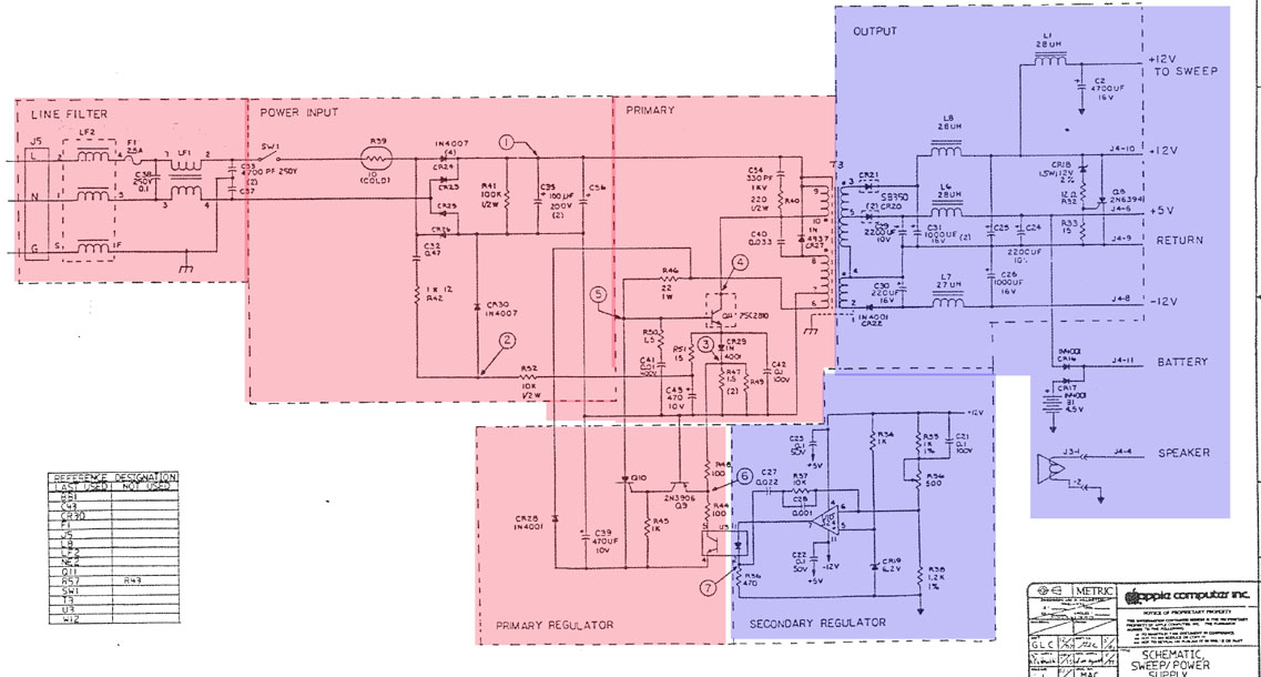
WARNING
: At the following circuit diagrams i have marked up with
light red shading the so called
"primary side" of the supply. In this areas there are
voltages up to 400 Volt present!
Such voltages are
lethal dangerous !
Never access this areas with present "live Voltage" ( i.e. supply
"powered up" ) !
Red highlighted areas may only be accessed while
powersupply is disconnected
from main powersource ( disconnected from powercord ) !
Never attempt this areas without ensuring the demanded
precautions of safty !
Only experienced Users with advanced knowledge and
successfully solved safty training
may work at this red highlighted areas !
Read red colored text with safty warnings ! Do not ignore this
warnings !
Ignoring this warnings may cause electric schock with lethal
results !
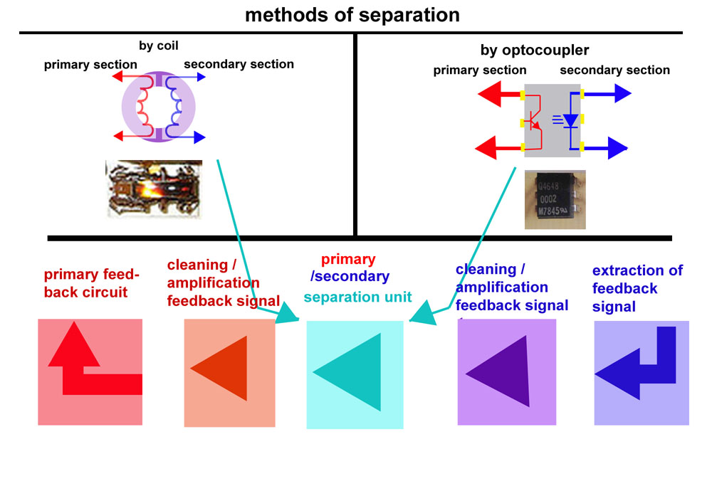
For security reasons in nearly all powersupplies it was
common habit to have a kind of "separation method" to keep
strict
the primary section apart from the secondary section. The 2
most common methods used have been using either a coil-
separation or a optocoupler, where the LED side was
connected to secondary side while phototransistor was
connected to
primary side. The picture below displays left side the coil
method and right side the optocoupler method and picture of
the
seperations units themselves.
 |
The feedback path may be explained in
simple functions:
Pick signal from secondary voltage path to be used as feedback signal,
clean that signal from disturbing dirt, maybe some small amplification
for use at the seperator ( voltage level )
seperated transmission to isolated other primary side,
cleaning the feedback signal and amplification for use in primary side,
injection of the feedback signal to control/regulation circuit at the
primary side.
For use as feedback signal there have been 2 variable parameters to take
influence to the primary section and
thereby controlling the secondary section:
length of positive puls to control secondary amount of current ( i.e.
how much ampere )
and frequency used in transformer to control voltage level ( i.e. how
many volts ).
Some feedback paths instead seperated "dirtsignal" from secondary
section and pushed that signal back to primary section
targeting to eliminate the "dirtsignals" at secondary side ( similar to
audio amplifiers ), by adding a inverted dirtsignal at the
primary section with pupose to "eliminate" dirtsignal by compensation.
This kind of control was rather more rare and therefor
will not be explained here.
In generaal the first kind of feedback was used to keep control to the
transmissionprocess from primary section to the secondary
section to avoid waste of power and keep amount of "powerconsumption"
low ( not wasting unused power ).
Just to explain visually the previously explained example options of
control by feedback by control of the
voltage switching by the powertransistor at the maintransformer:
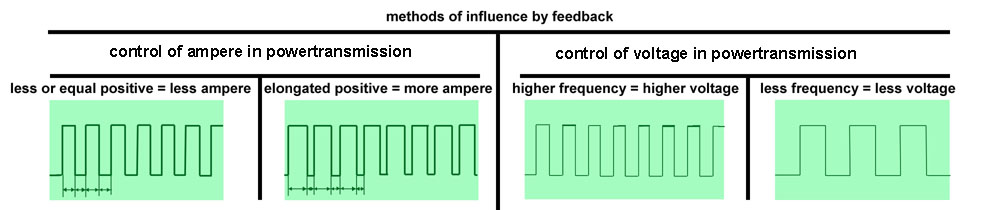 |
In fact the range of control is ( not like in the picture above
) not that large..... the true range of variation to execute control
is limited to maximum of aproximatly only +/- 15% !
 |
Now lets take a view to the details of a
typical feedback path with an optocoupler:
In this plan the seperation circuit is a optocoupler NEC2501.
We´ll take our focus
to the secondary part of the feedback trail.
The LED part of nearly all optocouplers use the voltage and
powerregulation chip
TL431 to ensure that the "basic
setup" of the LED has a kind basic brightness and
lightemmision. The path A
still contains a portion of squarewave signal taken from
the supplybranch at the transformer side E before it
passes the filtering coil ( choke ).
This squarewave portion will cause a kind of flickering at the
LED in the frequency
used at the transformer in the secondary section.
After the choke at position F the supplyvoltage is cleaned from
that portion of squarewave
voltage. The path B measures behind
the resistor R2 the amount of
ampere flowing along
the supplytrace to the connected device ( i.e. Mainboard ) and
besides also adding the small
portion of AC "dirtvoltage" of the final voltagesupply to the
compensation measurements
and also affecting the lightemmision of the LED , while the path
C is used to
measure the voltage at that powertrace by taking a fixed portion
of voltage between the
resistors R4 and
R5 and adding that amount of
voltage to the "base connector" of the
TL431
and therefor slightly causing a variety in brightness of the LED
above of the TL431.
The capacitor C9 blocks the DC
voltage in the path C to the
connection of the path B and
is only passed by AC "dirtvoltage" portion of the
supply-voltage.
In this kind of feedback you will allways be able to identify
the typ of feedback by the presence
of some kind of 6 pin device as optocoupler and in most cases
added to that ( the transistor alike
looking ) 3 pin case of the IC TL431. The points that change
from different powersupplies
are the components between the "transmission"unit consisting of
the optocoupler and the TL431
and the components added in between that units and the measuring
points at the traces picking
the voltages to be measured.
|
While path
B measures amount of current (ampere) passing along the
path of - 5 Volt, the path C
measures voltage at - 5 Volt rail and path
D measures the Voltage of + 5 Volt rail. |
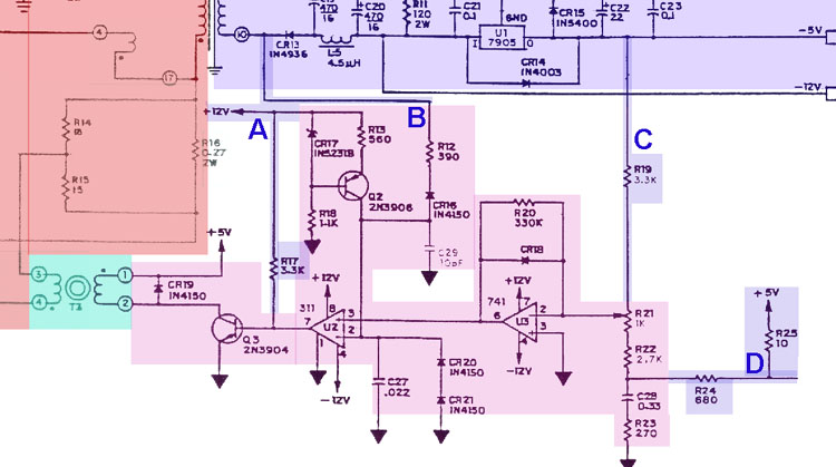
Now lets take a view to the details of a
typical feedback path with a coil:
The voltage in Path A taken
from +12 Volt path is regulated and therefor
is only used for "pullup" of the base of
Q5. The
Q5 in
fact gets its signal from the output of
the comperator 311 (
U2 ).
The one reference of the comparator is resulting from path of
B
by the Path CR17 and
R18 at the base of transistor
Q2 and the emitter of
Q2 with R15
setting up the defined voltage at the emitter and at the
alternate variable path of B
getting the
squarewaves from the - 5 Volt coil
passing R12 and interacting with
CR16 and C25
picking the small rest of the disturbing
"dirt-voltage" at the junction of R15
and CR16 and
adding
that voltage up to the reference at the
collector of Q2 to
the fixed reference made by the 2 diodes
CR20 and CR21 together with
C27. This is compared
to the predefined voltage
at the output of the 741
OPamp. The "setting" of the 741
OPamp is resulting from path C
taken from the -5 Volt trace
behind the regulation along the
R19 resistor, the trimming resistor
R21, and the 2 remaining resistors
R22 and R23.
C25 is just blocking a portion of
the DC voltage and passes part of the remaining frequent
"dirt-voltage" to the Ground while other part of the measured
voltage is taken from Path D by the
resistor R24 to the "hot" end (
positive end ) of the trimming resistor
R21. |
later a powersupply became common that had additional regulation /
adjustment section:
And more sophisticated the powersupply of the IIGS with quite complex
feedback sections:
|
|