Apple I Replica Creation -- Chapter 4: Building the Replica I
| Chapter 4 |
| Building the Replica I |
Introduction
Before learning microcomputer design, it helps to know how to program, and before learning how to program, it's best to have a computer with which you can program. This chapter will discuss building the Replica I with a minimum of theory. First an introduction to soldering will be provided. This will be followed by step-by-step instructions for assembling the Replica I kit sold by Vince Briel and a discussion of the Serial I/O board. Finally, the McCAD EDS package will be introduced for readers interested in having their own boards fabricated.
Learning to Solder
Soldering is a skill that takes time to learn. If you've never soldered before, I would suggest acquiring some practice time before attempting to assemble the Replica I. Test your skills on old circuit boards by removing components and putting them back in, or buy a couple of cheap parts from Radio Shack on which to practice.
The first time you use a new soldering iron, you need to tin the tip, which is done by heating the iron and applying a thin coating of solder to the tip. The surface and components you are about to solder must be clean. With a new Replica I board, this is not a concern, but if any of your parts are older or appear dirty, clean them with steel wool or alcohol.
Insert the component you wish to solder into the board; in this example we will use a resistor. Identify the correct location for the part and insert it, bending the leads as necessary to make it fit. Flip the board over and bend the resistor's leads slightly outward so that it will stay in place.
Allow your soldering iron to fully heat up before starting. Place the tip of the iron so it touches both the lead and the hole (Figure 4.1). Both must be hot for a reliable connection. Hold the solder so that it touches both the lead and the hole, but not the soldering iron. In a second or two the solder will start to flow. When the hole fills and begins to look like the solder joints you've seen on commercially-made boards, stop applying solder. This will probably take no longer than a second.
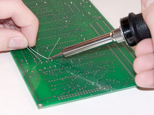
Figure 4.1 Applying Solder
Allow a few seconds for the solder to cool. Then, cut off the excess lead (Figure 4.2). Be careful not to jostle the joint before it is cool or you risk damaging the connection.
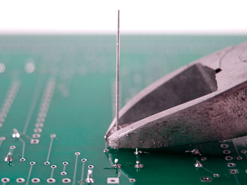
Figure 4.2 Trimming the Leads
Figure 4.3 shows some finished solder joints. Your joints should be shaped like these with a shiny and smooth finish. If your joint is dull and dirty, you have a cold solder joint—possibly because you bumped the joint while the solder was still cooling or because the joint is not getting hot enough. Though the connection may look solid, it is not electrically reliable and should be resoldered.
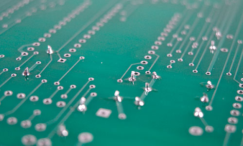
Figure 4.3 The Finished Joints
Assembling the Replica I
Figure 4.4 shows the unassembled Replica I kit available from Briel Computers. Included with the kit is all the parts you'll need to build a working Replica I. If you're a more advanced user, Briel also sells components individually, which allows you to mix and match parts or install them on your own printed circuit board, described later in this chapter. Users uncomfortable with soldering can order pre-assembled kits.
Assembling the Replica I TE The instructions in this section describe building Briel Computers' original Replica I. This original kit has since been replaced by the Replica I TE. If you have the new TE model, you might still find this chapter useful for soldering and assembly tips, but don't use it determine the placement of specific components. Of particular note is that the Replica I TE has an onboard serial interface, so there is no longer any need for the Serial I/O Board. |
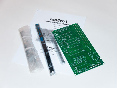
Figure 4.4 The Unassembled Briel Replica I Kit
Parts List
These are the parts included with the Replica I kit, other than the bare printed circuit board.
ICs:
- 6502 CPU 40-pin IC
- 6821 PIA 40-pin IC
- 28C64 EEPROM 28-pin IC
- 62256 SRAM 28-pin IC
- 74LS00 TTL 14-pin IC
- 74LS04 TTL 14-pin IC
- 74HC74 TTL 14-pin IC
- 74LS138 TTL 16-pin IC
- 74HC166 TTL 16-pin IC
- ATMEGA8 28-pin IC
- ATMEGA8515 40-pin IC
Crystals:
- 14.31818 MHz Crystal
- 8.0 MHz Crystal
- 1 MHz TTL Clock
Sockets:
- Qty 3—40-pin
- Qty 2—28-pin (wide)
- Qty 1—28-pin (narrow)
- Qty 2—16-pin
- Qty 1—16-pin (spring socket, for ASCII keyboard)
- Qty 3—14-pin
Connectors:
- Qty 1—40-pin Expansion Header
- Qty 1—DIN PS/2 Keyboard Connector
- Qty 2—Power Supply Connectors
- Qty 1—Video Connector
Resistors:
- R1: 1.5 K Ohm (brown-green-red-gold)
- R2: 470 Ohm (yellow-magneta-brown-gold)
- R3: 100 Ohm (brown-black-brown-gold)
- R4, R5: 4.7 K Ohm (yellow-magneta-red-gold)
- R6–R10: 3.3 K Ohm (orange-orange-red-gold)
Capacitors:
- C1, C2, C4, C4: 18 pF
- C3: 0.1 µF
- C6–C17: 0.1 µF Bypass
- C18: 0.01 µF
Diodes:
- D1, D2: 1N4148
Other:
- Qty 2—Button
- Qty 1—Jumper Pad
Resistors
It's easiest to install smaller components first. This way, when you turn the board over, the component will be held in place between the table and the board. Let's install the resistors first. There are ten resistors on the Replica I board labeled R1 through R10. These labels are silk-screened onto the Replica I's printed circuit board, making it easy to determine where parts should go. In the case of resistors, the resistor value is shown beneath the label (Figure 4.5). You can check these values using the table of resistor codes in Chapter 3.
Polarity does not matter for resistors—you can install them in either direction. For the sake of aesthetics, I like to place all of mine in the same direction. With all resistors installed, your board should look like that in Figure 4.6. If you have doubts about the quality of your soldering, use a multimeter and measure across the resistors, solder joint to solder joint.

Figure 4.5 Resistors
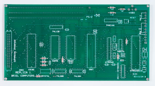
Figure 4.6 Installed Resistors
Diodes and Bypass Capacitors
Next, install the two diodes at D1 and D2. For these, polarity does matter. The negative (cathode) end of the diode is indicated by a black ring, and the negative end on the board is indicated by a square pin. Match these up when installing the diodes. You can also refer to the silk-screened image between the pins, which illustrates where the ring should be. Figure 4.7 shows the two diodes properly installed.
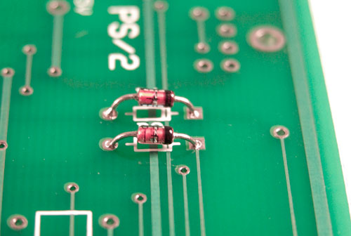
Figure 4.7 Installed Diodes
The 11 bypass capacitors (Figure 4.8) are as easy to install as the resistors. Polarity is unimportant. Bend the leads, solder them into place, and snip the extra length off.

Figure 4.8 0.1 µF Bypass Capacitor at C6–C17
Buttons
There are two buttons on the Replica I motherboard, one each for Reset and Clear (Figure 4.9). Polarity on these does not matter. Near each button you'll see a pair of holes for connecting an external button. If you're installing your Replica I in a case, you'll probably want to do this. The wires from the external button can be soldered directly to the board, or a socket can be used. Figure out what sort of external button you'll be using before doing anything with these.
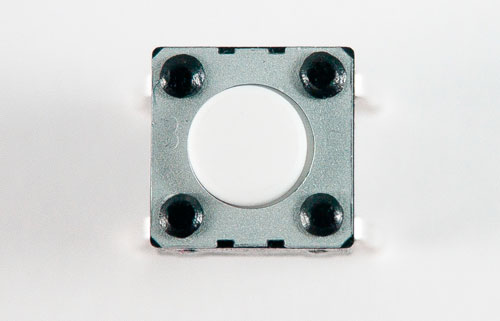
Figure 4.9 Button
Sockets
Sockets should be installed such that the notch shown in the silkscreen matches the notch in the socket (Figure 4.10). Pin 1 on the circuit board is also indicated by a square pin. If you have trouble holding the socket in place while you turn the board over to solder, try temporarily taping it down.
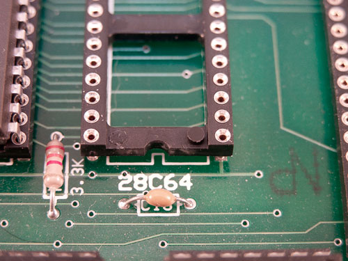
Figure 4.10 Socket Orientation
ASCII Keyboard Socket
The ASCII keyboard connects via a spring socket (Figure 4.11), which looks slightly different than the machined sockets used for the chips. A spring socket is used here because it's easy to connect and disconnect the keyboard connector from it. Machined sockets are generally of higher quality, which is why they're used for the rest of the board. If you're going to be using a PS/2 keyboard exclusively, you can skip installing this part.

Figure 4.11 ASCII Keyboard Socket
Capacitors
The capacitors are not polarized. Installing them is trivial once you've learned to distinguish one type from another. Figure 4.12 shows the 0.1 µF capacitor used in C3. The 18pf capacitor in Figure 4.13 is for locations C1 through C5. Figure 4.14 shows a 0.01 µF capacitor which belongs at C18.
 Figure 4.12 0.1 µF Capacitor for C3 |
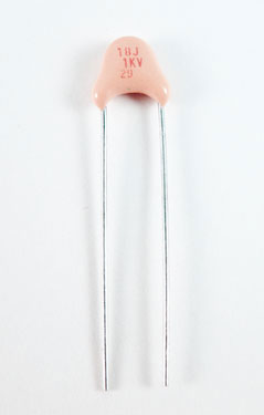 Figure 4.13 18pF Capacitor for C1–C5 |
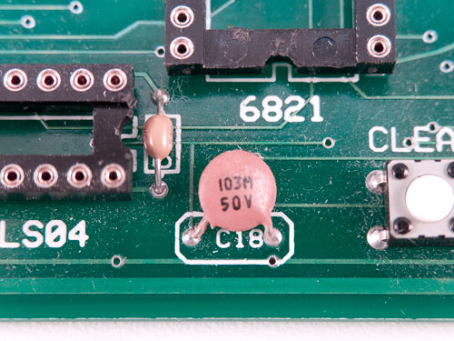
Figure 4.14 0.01 µF Capacitor for C18
Header and Jumper
The 40-pin expansion header should be installed so that the single notch faces outward, away from the board, and the double notches face inward, towards the board. The double notches are towards the top in Figure 4.15.
The jumper pad (Figure 4.16) has no polarity and should be installed at location JP1. The shorter end of the pins should be soldered to the board; the longer end should be facing up, away from the board. The jumper pad is used for switching between PS/2 and ASCII keyboard modes. If you're using an ASCII keyboard, a shorting jumper should be placed across the pins. Leave the pad unshorted in order to use a PS/2 keyboard.

Figure 4.15 40-Pin Expansion Header
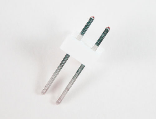
Figure 4.16 Jumper Pad
Crystals
The crystals are easy to damage and should be installed with care. The polarity of the 1 MHz TTL clock (Figure 4.17) is critical. Pin 1 on the clock is indicated by a black dot and a squared corner (the rest of the corners are rounded off). On the circuit board, pin 1 is indicated by a square pin while the rest of the pins are round. The 1 MHz clock should be installed at the location labeled OSC, for oscillator.
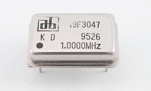
Figure 4.17 1MHz TTL Clock
For the other two crystals, polarity is unimportant. The 14 MHz crystal (Figure 4.18) should be installed next to the ATMEGA8 IC at the location labeled Q1. The 8 MHz crystal (Figure 4.19) should be installed beside the ATMEGA515 IC at location Q2.
 Figure 4.18 14MHz Crystal |
 Figure 4.19 8MHz Crystal |
Connectors
Almost done! The PS/2 connector (Figure 4.20) should be installed at the PS/2 label. Likewise, the video connector (Figure 4.21) should be installed at the video label. Both of these fit in only one way. The holes for the video connector are large. Be sure the entire hole is filled with solder for a secure electrical connection.
 Figure 4.20 PS/2 Connector |
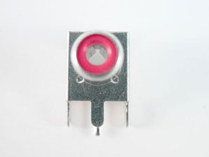 Figure 4.21 Video Connector |
Finally, install the power connectors. The two connectors are identical and thus interchangeable, but remember that orientation is important. The flat white support edge should be against the edge of the circuit board with the pins on the inside, as shown in Figure 4.22. When soldering these into place, I recommend using tape. The holes for the power connector's pins are large and it's easy for the connectors to slide around. Your finished board will look much nicer if the two connectors are neatly lined up.

Figure 4.22 Power Connectors
Finishing Assembly
Congratulations! You've completed all of the soldering. Now, all that remains is to install the chips. Each chip and each socket is labeled; it should be evident where the chips belong. Make sure you get the orientation correct—the notch on the chip should match the notch on the socket. Gently press the chips into their sockets and ensure that no pins are bent out of place.
When you've completed the preceding steps, connect the power cables. The black wires should be on the inside to match the silk-screened label of GND (Figure 4.23). Connect your monitor and keyboard. Make sure the keyboard select jumper (JP1) is set correctly for your keyboard. Step back and admire your masterpiece (Figure 4.24). Turn on the power and press Reset. A \ prompt should appear on the screen, which means you're ready to move on to start programming.
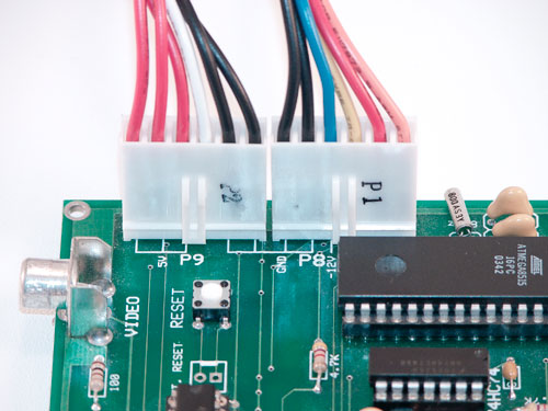
Figure 4.23 Connected Power
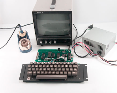
Figure 4.24 Completed Replica I System
Serial I/O Board
The Serial I/O board by Briel Computers (Figure 4.25) provides an easy way to interface the Apple I to a modern computer. The I/O board allows emulation of the keyboard and mouse using a terminal program on your Mac or PC. The board plugs into the 6821 socket and provides a standard nine-pin serial interface. Sending data to this serial port is the same as typing it on the keyboard. All data that is sent to the video section is also sent out the serial interface.
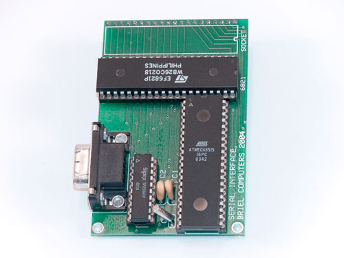
Figure 4.25 Serial I/O Board
To connect the I/O board, first disconnect all power. Next, use a small screwdriver to gently pry the 6821 out of its socket (Figure 4.26). Alternate between gently prying each side so as not to bend any pins. Do not use an IC puller to remove the chip, as this will put stress on the socket connections. Next, gently insert the Serial I/O board into the socket. In the Replica I, the nine-pin serial port should face the same direction as the video and PS/2 ports. The installed board is shown in Figure 4.27.
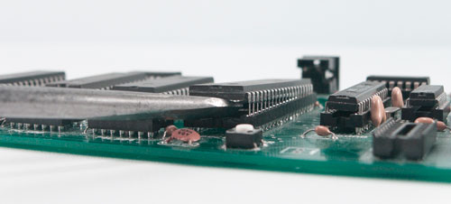
Figure 4.26 Removal of the 6821
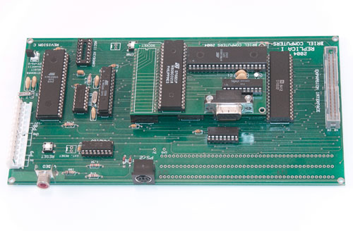
Figure 4.27 Serial I/O Board Installed
If you ever need to remove the serial board, be very careful. It pins are brittle and will easily snap off if bent too far. It is very easy to end up with a pin stuck in your socket that will be extremely difficult to remove.
If you have an older PC or Mac, the Serial I/O board can be connected directly to your computer's serial port via a straight serial cable (not null-modem cable). Newer computers will require a USB-to-serial adapter. One such adapter is the Keyspan USB Serial Adapter (#USA-19). The communication needs of the Apple I are very basic; consequently, any USB adapter that isn't special-purpose should work.
Windows users can use HyperTerminal, which is included with the operating system. Macintosh users will want to check out ZTerm by Dave Alverson. When launching ZTerm, hold down the Shift key. This will produce a menu where you can choose which serial port to use. If you're using the internal serial port on an older machine, you'll want to select "printer" or "modem" port. With a USB adapter, the name will be something obscure such as "USA19191P1.1."
Once the program is launched, choose Connection from the Settings menu and confirm that all your settings match those in Table 4.1. All other settings can be left at their defaults. Make sure your replica is running and has been reset. Text you now type in the terminal will be sent to the Apple I and video output will be sent to the terminal. Programs, available from the Apple I Owners Club on Applefritter, can be entered by simply using copy and paste in the terminal or by going to the File menu, selecting Send Text, and choosing the file that contains the program.
| Property | Setting |
| Data Rate | 2400 bps |
| Data Bits | 8 |
| Parity | None |
| Stop Bits | 1 |
| Echo | Off |
| Xon/Xoff | Off |
| Hardware Handshake | Off |
Using NVRAM Nonvolatile RAM (NVRAM) can be used in lieu of static RAM (SRAM) in your replica. NVRAM preserves the contents of memory, even when the computer is turned off. This means that programs you enter by hand will still be accessible the next time you use your replica. NVRAM is implemented either by placing a battery inside the IC to provide constant power to standard SRAM, or by using an EEPROM. The DS130Y-120 is an equivalent replacement for the 32 KB SRAM IC that is used normally in the Replica I. It's available from Digi-Key and others for about $20. |
Using McCAD EDS SE500
McCAD EDS SE500 is an electronic design system that includes all the tools you need to take a design from idea to production. Available on the Mac App Store, it's a package that includes Schematics SE500, PCB-ST SE500, and Gerber Translator. Schematics SE500 is a very easy-to-use program. The schematics it generates can be used with PCB-ST SE500, a PCB layout design environment, to design a printed circuit board based on the schematic. McCAD Gerber Translator will convert the PCB-ST document to a standard Gerber photo-plotting text command file that can be read by PCB manufacturers anywhere.
If you are new to circuit design, the circuits shown in this section will probably look foreign to you until you read the following chapters. It will be of interest to readers wishing to modify the Replica I circuit to suit their own needs and interests. Don't be fooled by the simple appearance of the McCAD interface. This is a very capable toolset that is easy to master yet very robust in its capabilities.
Documentation for McCAD EDS in PDF can be found in the application's Help menu. You are encouraged to read through the documentation before attempting a new design or modifying the files provided in the Supplemental Software package. If you run into difficulty, visit the forums on Applefritter at www.applefritter.com/forum.
McCAD Schematics SE500
Figure 4.28 shows the Replica I circuit opened in McCAD Schematics. The circuit can be modified using the tools on the left of the screen. Components selected from the Library menu can be placed and new components can be created using the online library editor. A separate library of Apple I components (6502, 6821, etc.) was created for inclusion with this book.
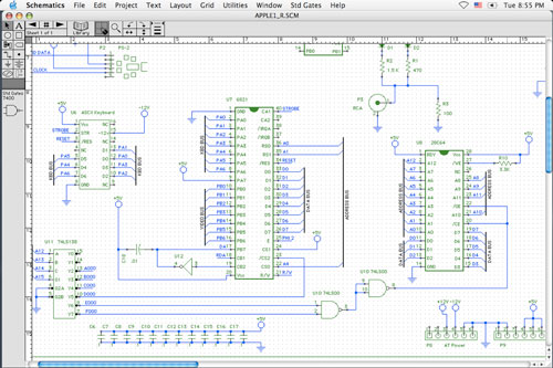
Figure 4.28 McCAD Schematics
McCAD PCB-ST SE500
Figure 4.29 shows the Replica I PCB open in McCAD PCB-ST. When you import a McCAD Schematics file to PCB-ST it will automatically collect the needed parts and allow you to place them and route the interconnecting traces. If you are happy with the Replica I circuit design but perhaps wanted to change the component layout or board shape, you would do so with this software. The standard Gerber file generated by PCB-ST can be sent to any PCB manufacturer to be fabricated.
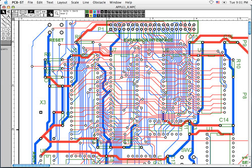
Figure 4.29 McCAD PCB-ST
| ← Previous | Contents | Next → |
