Apple I Replica Creation -- Chapter 7: Understanding the Apple I
| Chapter 7 |
| Understanding the Apple I |
Overview
The design of the Apple I is as simple and straightforward as any computer you'll find. Look at the block diagram in Figure 7.1. At the center of the design is the processor, the brains of the operation. All data passes through it, and it controls which data that is, and when. The ROM contains the Monitor, which, as you learned in the previous chapter, is essentially a very simple operating system. When the computer is first turned on, the processor immediately goes to the ROM and runs the Monitor program. The RAM is used to store user programs and data. You'll note that there is no mass storage device (hard drive, floppy drive, etc.) in this diagram or in the Apple I, though it would be possible to add one.
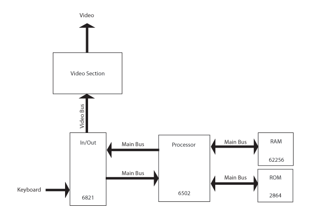
Figure 7.1 Apple I Block Diagram
Once the computer boots, it outputs a command line prompt (a slash) to the screen. The processor sends the character to the Input/Output (I/O) chip. The I/O chip waits until the video section is ready for the next character, then sends it off. The video section converts the character from digital data to an analog signal suitable for a video monitor. Input comes from the keyboard, where it is stored in the I/O chip and then transferred to the processor. It's very important to understand that the processor does all the work and directs all operations.
In this chapter, we'll discuss the workings of the processor, RAM, ROM, and I/O. The video section will be addressed briefly, but we will not cover the complexities of adapting the data for output to a CRT. Our emphasis will be on the digital workings of the computer.
The Data Bus
The Apple I's main components are all attached to the 8-bit data bus (Figure 7.2). All the data the processor sends or receives travels over this bus. The individual components cannot communicate with one another directly—all data must pass through the processor.
Let's say we have a character (we'll make it 'J') in RAM and we want to send it to the display. An ASCII character is a single byte, so it fits perfectly on our 8-bit data bus. Our first step is to get the data out of RAM and load it into the processor. We know the location, or address, of the character, so we put that location on the address bus. If the address were $2100, for example, the instruction would be LDA $2100.
Each device on the bus sees that address. The ROM and I/O chips look at the address and see that it's not for them. The RAM chip recognizes the address as its own and knows to which location in its memory that the address refers. The RAM chip looks at the Read/Write line to see whether the processor wants to read a byte from this address, or write a byte to it (that is, whether to load the 'J' into the processor or to overwrite the 'J' with some other letter). The Read line is high, so the RAM chip places the 'J' on the data bus, where it's then loaded into the processor.
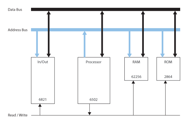
Figure 7.2 Data Flow
Next, we want to send the data from the processor to the video output via the I/O chip. A specific address on the I/O chip is associated with sending data to video-out. The processor puts that address on the address bus. The I/O chip recognizes that address as its own, the one intended for video-out data. The other chips don't recognize the address and thus ignore it. The Read line goes low (which means write), so the In/Out chip knows it will be receiving data and the character 'J' is placed on the data bus. At the clock pulse, the I/O chip reads the data off the data bus. Then the I/O chip sends it off to the video circuitry.
The Address Bus
The address bus is 16 bits wide, which means we have enough addresses for 65,536 (64K, or 216) unique locations. Usually, these locations are memory addresses (RAM), but they could range anywhere from light emitting diodes (LEDs) to sensors or I/O chips. Let's say we have a 32-kilobyte RAM chip. Half of our available addresses fit within 32K, so let's make this chip occupy the lower half of the address space, addresses 0 through 32,767. Whenever the address is 32,767 or less, we want to enable the chip. How can we check for numbers in this range?
One very complex possibility is to check each possible combination. For example, to check for 1, which is within our range, we would write:
Enabled for 1 = A15' • A14' • A13' • A12' • A11' • A10' • A9' • A8' • A7' • A6' • A5' • A4' • A3' • A2' • A1' • A0
Or to check for 14,287, which is also within our desired range, we would write:
Enabled for 14287 = A15' • A14' • A13 • A12 • A11' • A10 • A9 • A8 • A7 • A6 • A5' • A4' • A3 • A2 • A1 • A0
And we would end up doing this 32,767 times, once for each address. This approach would certainly work, but the amount of work and time needed to complete the task would be so enormous that it would be terribly impractical. Let's try to find a simpler method by examining the relevance of each bit. The lowest bit, A0, alternates high and low with each number, so it's no good for determining whether a number is larger or smaller than 32K. The same applies to bit A1, which alternates high and low with every second number. Let's look at the range of numbers we have to cover (Table 7.1):
| Decimal | Binary |
| 0 | 0000 0000 0000 0000b |
| 32,767 | 0111 1111 1111 1111b |
Notice from this table is that although bits A14 through A0 change, bit A15 is always 0. Not only that, but our range includes every number where A15 is 0. If A15 is low, we know the address is within our 0 to 32K range. Our circuit, shown in Figure 7.3, is now trivial—whenever A15 is low, enable the chip.
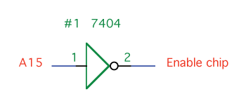
Figure 7.3 32 KB Enable
You might be thinking that this example was contrived to work out easily, and it certainly was, but that doesn't make it unrealistic. Any memory chip you find is going to be based on a power of two, and when you're designing a computer, it certainly behooves you to use start and end points that are easily defined in logic.
Let's take a harder example. Suppose we have 16 kilobytes of RAM and we want to locate this memory at addresses 32K through 48K. Our table would then look like Table 7.2:
| Decimal | Binary |
| 32,768 | 1000 0000 0000 0000b |
| 49,151 | 1011 1111 1111 1111b |
Bits A0 through A13 will vary, so we can disregard those for now. A14 must be 0, because if it were 1, the value would be larger than 48K. A15 must be 1, because if it were 0, the value would be smaller than 32K. Thus, we want to enable our chip whenever A15 is high and A14 is low (Figure 7.4).
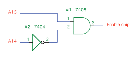
Figure 7.4 16 KB Enable
Now that we've enabled the chip we want to use, we need to identify the location on that chip. This is where the rest of the address lines on the address bus come into play. Bits A0 through A13 can express our entire range of locations. These lines are connected directly to the address lines on the chip so that it can find the internal location of the requested data.
Bidirectional Buses The data bus is bidirectional, meaning that data can be both sent and received over it. The Read/Write line is used to determine which direction the data is going. The address bus, by contrast, is unidirectional. Only the processor can send data to it. The rest of the chips (such as RAM, ROM, and others) can only read what's on the address bus. |
The Clock
Everything happens at the clock pulse. New values are waiting at the register inputs. When the clock pulses, the new values are loaded into the registers over the course of a couple nanoseconds, then become present at the output of the registers. The output signal propagates through the circuit, each logic gate taking a few more nanoseconds. Eventually, all is updated and the lines stabilize. At this point, the clock pulses and the cycle repeats. Figure 7.5 shows a 1MHz TTL crystal oscillator, which we will use for our clock.
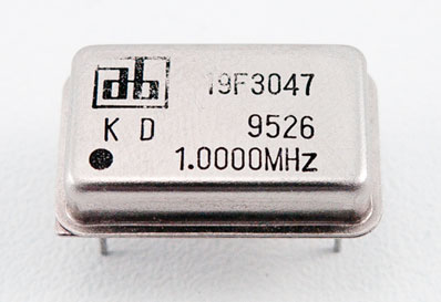
Figure 7.5 1MHz TTL Crystal Oscillator
Figure 7.6 shows a timing diagram for the clock pulse. At each rising edge, indicated by an arrow, the circuit updates. The Apple I uses a 1MHz clock. Compare that to the multi-gigahertz clocks in today's computers, and it's glacially slow. What would happen if we put a 1GHz clock in the Apple I? At 1GHz, the circuit would not have time to fully propagate after each clock pulse, leaving the circuit partially updated and in an uncertain state.
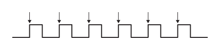
Figure 7.6 Timing Diagram
Figure 7.7 shows the pinout for a 1MHz TTL crystal oscillator. Pin 1 is not used. Pins 7 and 14 are ground and power, respectively. Pin 8 is our clock output. The output is low for 500KHz, then high for 500KHz. Our circuitry triggers on the rising edge.
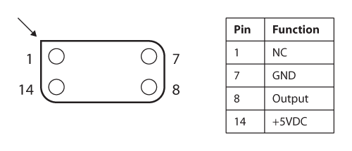
Figure 7.7 1MHz TTL Crystal Oscillator Pinout
The Processor
Fully understanding the operations of the 6502 processor (Figure 7.8) sounds daunting, and it certainly could be. However, we're going to concentrate on understanding the processor from the user's perspective, which simplifies our cause. You won't learn how to build a processor from scratch (that's another book in itself), but you will learn how to design basic circuits that interact with the processor. In Chapter 6, we discussed how to write programs in machine language that can be directly understood by the 6502. This chapter will go into more depth, looking at what happens when you run those programs.
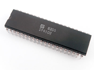
Figure 7.8 6502 Microprocessor
Pins and Descriptions
The 6502 (Figure 7.9) comes in a 40-pin dual in-line package (DIP). The function of each pin is described later in this chapter. If you're using the slightly newer and more advanced 65c02 chip, you'll have a few extra features available. These features aren't used by the Apple I, and the 65c02 is backwards compatible with the 6502, so you can safely think of your 65c02 as an ordinary 6502 processor.
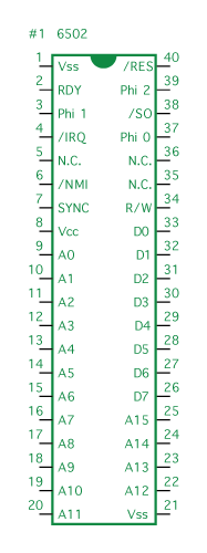
Figure 7.9 6502 Pinout
Address Bus (A0-A15)
The address bus is a 16-bit bus capable of addressing 64 kilobytes. Those bytes could be locations in memory or on input/output devices.
Clock (φ0, φ1, φ2)
The symbol φ0 (or Phi 0) denotes the oscillator input. Connect the output of your 1MHz clock to this line. φ1 and φ2 are outputs that are offset from this clock line. φ1 is not used by the Apple I. φ2 is used when writing to the 6821 PIA and the RAM.
Data Bus (D0-D8)
The eight-bit data bus allows bidirectional communication between the processor and memory or other peripheral devices.
Interrupt Request (IRQ)
This line is not used by the Apple I. A pulse on the interrupt line tells the processor to stop what it's doing and to process data from another location.
No Connection (NC)
There is no signal on this line; as a result, it can be left disconnected. If you're using the later 65c02 instead of the original 6502, you'll find some of the NC pins have been replaced with actual signals. The 65c02 is backward-compatible, so you can just leave these lines disconnected as you would on the 6502.
Non-Maskable Interrupt (NMI)
This line is not used by the Apple I. Whereas a normal interrupt (IRQ) can be blocked by software, a non-maskable interrupt will always succeed in getting through and interrupting the system.
Ready (RDY)
This line is not used by the Apple I. The Ready line allows you to halt or single-step the processor. This can be especially handy if you're trying to troubleshoot a design and want to see what the system is doing, one step at a time.
Reset (RES)
When power is first applied to the processor, it's in an unknown state. Pressing the Reset button tells it to load the program at the address contained at $FFFC and $FFFD and to start executing.
Read/Write (R/W)
The Read/Write line is used in conjunction with the data bus. When Read is high, the processor is reading data from the data bus. When Read is low, the processor is writing data to the data bus.
Set Overflow Flag (SO)
This line is not used by the Apple I. Its function is to manually set the overflow flag in the processor. The overflow flag is used to indicate that a number is larger than can be contained.
Sync
This line is not used by the Apple I. Sync can be used in combination with RDY to single-step the processor.
Voltage Common Collector (Vcc)
Vcc is the positive voltage line. It provides power for the chip and connects to the five-volt signal.
Voltage Source (Vss)
Vss is the ground line. The 6502 has two Vss lines, probably for additional current-handling.
With this knowledge, we can draw the schematic for the processor (Figure 7.10). The address lines go to the address bus, and the data lines to the data bus. The Read/Write, Phi 0, and Phi 2 pins are all wired to their respective lines. /SO is disabled by being tied to high. RDY, /IRQ, and /NMI are tied to high with current-limiting resistors. Reset is connected to the reset circuitry, which is high until the switch is depressed.
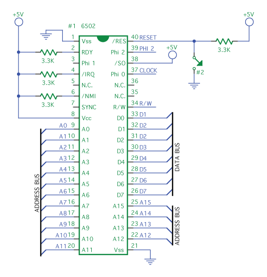
Figure 7.10 Processor Schematic
Registers
Registers, discussed in Chapter 5, are a fundamental part of the microprocessor. Each data register in the 6502 has a capacity of eight bits, and can therefore store an entire byte of data. The Program Counter (PC) can hold 16 bits. Registers allow the processor easy access to the data it needs to operate. Figure 7.11 shows the five registers most important to us.
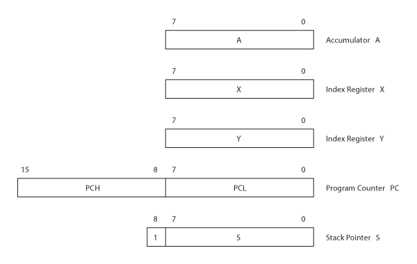
Figure 7.11 6502 Registers
The Accumulator
The Accumulator is used for mathematical and logical operations. If you have a number on which you want to perform addition or subtraction, you first load it into the Accumulator.
Index Registers X and Y
X and Y are generic registers. If you have a byte of data that you just want to keep nearby or are moving from one peripheral to another, the X and Y registers are convenient nearby storage places. It's also very easy to move data between various registers, so if you have a byte in X that you want to do a mathematical operation upon, you can easily transfer it to the Accumulator.
Program Counter (PC)
The PC is a 16-bit register used for keeping track of the address of the current instruction. It is incremented each time an instruction or data is fetched from memory. The processor looks at the program counter to see where it should fetch its next instruction.
Stack Pointer
The stack pointer points to (gives the address of) the current top of the stack. This address will change every time a byte is added or removed from the stack. The function of the stack is described later in this chapter.
Processor Status Register
The processor status register (Figure 7.12) is a collection of individual flags that serve as indicators for various instructions. For example, if you perform a subtraction and the answer is negative, the negative flag will be set. Then the next instruction can check that flag, see that the answer was negative, and report back to your program.
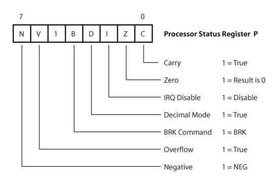
Figure 7.12 Processor Status Register
The Arithmetic and Logic Unit
The Arithmetic and Logic Unit (ALU) is at the heart of the microprocessor. The ALU can be thought of as a processing machine. Put the numbers you want to work on at the entry, choose the function you want, and let it run. The answer comes out the other end and is stored in the Accumulator.
The Stack
The stack lets us save data for future use. Access to data on the stack is limited. Only the topmost value can be read. Data is either "pushed" onto the stack or "popped" off of it. The stack pointer remembers the current location of the top of the stack. When data is pushed, the stack grows and the stack pointer is incremented. When data is popped, the stack shrinks and the stack pointer is decremented. Chapter 6 discusses how to program with the stack.
The stack uses memory from $0100 to $01FF (figure 7.13). $01FF is the base address. As data is pushed onto the stack, the stack grows towards $0100. The size of the stack cannot exceed the 255 bytes allocated to it.
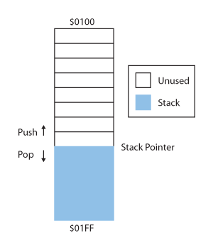
Figure 7.13 6502 Stack
Memory
Let's take a look at the way memory is used in the Apple I.
Where is It?
The Apple I has 64 KB of addressable space. The Monitor ROM occupies 256 bytes. The original Apple I also had 8 KB of RAM. Of the 64K addresses ($0000 through $FFFF), where should this memory be located? Deciding on a location for the ROM is easy. The 6502 microprocessor requires that a memory address be stored at addresses $FFFE and $FFFF (the address is 16-bit, so it takes two bytes). When the 6502 is reset, it immediately loads the address at $FFEF and $FFFF into its program counter and begins executing that address. Thus, you need to have a ROM at $FFFE–$FFFF, and if you need to have it there, you might as well keep the ROM in a solid block. The Monitor ROM, therefore, starts at $FF00 and ends at $FFFF.
The RAM, by contrast, is divided into two parts. Four kilobytes are for system and user access. These 4 KB are located at $000–$0FFF. The other 4 KB, which are intended for Apple's Integer BASIC, are located at $E000–$EFFF. You'll note that $E000–$EFFF are RAM, not ROM. Every time the original Apple I was powered up, the code for BASIC would have to be either loaded from cassette or typed in by hand. If the user did not need BASIC, he or she could refrain from loading it and just use that memory as generic memory space.
Figure 7.14 shows the memory map for the Apple I, as designed by Steve Wozniak.
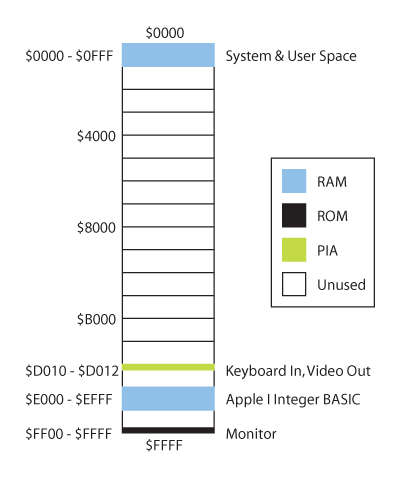
Figure 7.14 Apple I Memory Map
Note that the vast majority of this address space is unused. If the user wanted, he or she could expand the RAM in some of these blocks or use it for other peripheral devices. Joe Torzewski, who started the Apple I Owners Club in 1977, upgraded his Apple I to 16 KB. It would be possible to fill the entire unused memory with additional RAM.
Why did Apple include so little memory? Back in 1976, that 8 KB of RAM was prohibitively expensive. Today, by contrast, the price of RAM has plummeted, and the difference in cost between 8 KB and a hundred times that is negligible. Unless you're going strictly for historical accuracy, you'll probably want to add more RAM to your replica design. Figure 7.15 shows the memory map for Briel Computers' Replica I.
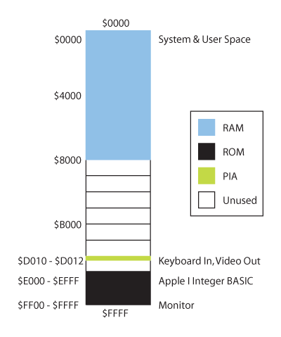
Figure 7.15 Replica I Memory Map
The first thing you'll notice about Briel's design is all the extra RAM. The first 32 KB ($0000–$8000) are all dedicated to system and user space. This is memory you're free to play around with. This is eight times the amount of system and user space in the original design, and that kind of expansion can make a big difference. Next, look at locations $E000 to $EFFF. Instead of being in RAM, Integer BASIC is now in ROM. This means BASIC is permanently stored on the Apple I and is immediately available when the system is turned on.
If you're a hardy assembly language programmer who scorns BASIC, this may be superfluous, but for everybody else, it saves a tremendous amount of time and frustration. Finally, note that addresses $F000 to $FE99 are mapped to ROM, but aren't labeled. If there's a program you use very frequently, you could potentially put it in ROM here, but right now, the space is wasted. Dedicating the entire 4 KB block, $F000–$FFFF, to ROM makes addressing easier and decreases the number of chips we need to place on the circuit board.
Implementing 8 KB RAM
The original Apple I used 16 MK4096 ICs to get 8 KB RAM. We can do the same with a single Cypress CY6264 (Figure 7.16). Let's briefly take a look at the function of the more interesting pins.
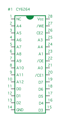
Figure 7.16 CY6264 Pinout
Address Lines (A0–A12)
You'll see that there are 13 address lines, which is enough to address 213, or 8,192, locations—conveniently, though not unintentionally, 8 KB. For the most part, these pins will be connected directly to the address bus, but there are some tricks we can play to divide the RAM into two separate blocks.
Data Lines (D0–D7)
All eight data lines are connected directly to the data bus.
Chip Enable (/CE1, CE2)
When Chip Enable 1 is low and Chip Enable 2 is high, the chip is "turned on" and will attempt to either read data from the bus or write data to it.
Write Enable (/WE)
When the chip is enabled and Write Enable is low, the data on the data bus is written to memory.
Output Enable (/OE)
When the chip is enabled and Output Enable is low, data from memory is output onto the data bus.
The difficulty in wiring up the RAM comes from having to divide it into two blocks, one at $0000–$0FFF and one at $E000–$EFFF. We must enable the chip only when the address on the address bus is within those ranges. The CY6264 has two chip enables. Both must be enabled to enable the chip. For simplicity, we're just going to use one (CE2) and tie /CE1 to ground so that it is always enabled. Since CE2 should be high for addresses in either range $0000–$0FFF or $E000–$EFFF, we can write the statement:
CE2 = ($0000 to $0FFF) + ($E00 to $EFFF)
Keep in mind that the + here means OR. Since the lowest 12 bits in each part of the statement can change without having CE2, we can rewrite the equation:
CE2 = ($0xxx) + ($Exxx)
Now we just need to look at the leftmost four bits, which represent pins A15, A14, A13, and A12. Converting 0 and E to binary, we get:
$0 = 0000b
$E = 1110b
Given that those binary digits represent pins A15 through A12, we can write the statements:
$0xxx = A15 ' • A14 ' • A13 ' • A12 '
$Exxx = A15 • A14 • A13 • A12 '
Then we put them together to realize our expression for CE2:
CE2 = (A15 ' • A14 ' • A13 ' • A12 ') + (A15 • A14 • A13 • A12 ')
The circuit created from this expression can be seen in Figure 7.17. The implementation of the latter half is straightforward (four signals, one inverted, going into a quad-AND gate). To implement the former half, we could have used four inverters going into a quad-AND gate, but instead we took advantage of DeMorgan's Laws to create an equivalent circuit using OR gates. Since four OR gates come to a chip, this approach lends itself to a more efficient design.
Our RAM chip will be enabled whenever an address on the address bus is within its range. We need to add some circuitry to the chip's address lines to make it map to two separate blocks. Since we have 8 KB and we want two blocks of 4 KB, we can use one of the address lines as a switch. A12 can be that address line. Let's make A12 high when the address is in the $Exxx region. A12 is low for every other region, but because our chip is only enabled for $Exxx and $0xxx, that effectively means A12 is only low for $0xxx.
When enabled, our memory chip is always either reading or writing data, as dictated by the processor's Read/Write line. The Read/Write line is high when the processor is reading and low when the processor is writing. We need to connect this Read/Write line directly to the Output Enable (/OE) line of memory. We also connect the inverted Read/Write line to the chip's Write Enable (/WE), but since we don't want to write until the data is available, we AND the inverted R/W with the Phi 2 clock, which is used for timing memory writes. Both lines are active-low (are activated by a low signal, as opposed to a high). "Output Enable" corresponds to "Read." Because Read/Write is low when the processor wants to write and Write Enable is active-low, we can hook the Read/Write line directly to the Write Enable pin. Whenever we're not writing, we're reading; consequently, Output Enable should be high whenever Write Enable is low, and vice versa. This means Output Enable should be hooked up to the inverted Read/Write signal. The complete schematic is shown in Figure 7.17.
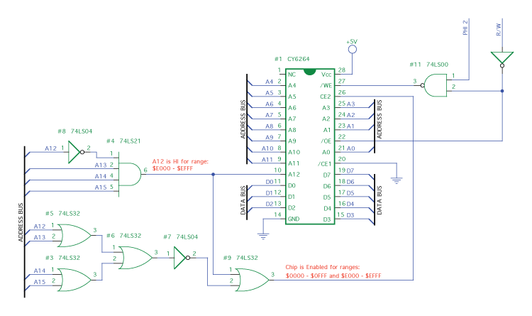
Figure 7.17 8 KB RAM Schematic
Dynamic and Static RAM The original Apple I was built using dynamic RAM, which is still prevalent in computers today. In dynamic RAM, each memory cell (one bit) is made up of a transistor and a capacitor. If the capacitor loses its charge, the content of memory is forgotten. A capacitor will discharge after just a couple milliseconds, so dynamic memory relies upon external refresh circuitry to keep the capacitor charged. Static memory, by contrast, uses a flip-flop for each bit. A flip-flop, of course, requires no refreshing, so static memory is a lot easier to work with. It's also faster. Unfortunately, a flip-flop is a lot more complex than a mere transistor and capacitor; therefore, static memory is a lot more expensive, which is why dynamic memory remains so common today. A static RAM chip of a few kilobytes costs only a couple dollars, so for our project it's perfectly economical. |
Implementing 32 KB RAM
The 32 KB RAM design used in the Replica I is far simpler than the 8 KB example we just examined. The chip used is a 62256 static RAM IC (Figure 7.18). The design for the 62256 mirrors our earlier example. The chip should be enabled whenever the lower half of memory is addressed. This occurs whenever A15 is low, giving us the result of CE = A15 . Our only chip enable line is /CE1, so /CE1 = A15, so this leaves us with the Write Enable and Output (Read) Enable lines to configure. Writing takes precedence if both Write Enable and Output Enable are true. Therefore, we can enable output whenever the chip is enabled. Write should be enabled when Read/Write is low and Phi 2 (the clock used for memory writes) is high. The completed design is shown in Figure 7.19.
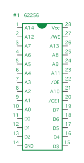 Figure 7.18 62256 Pinout |
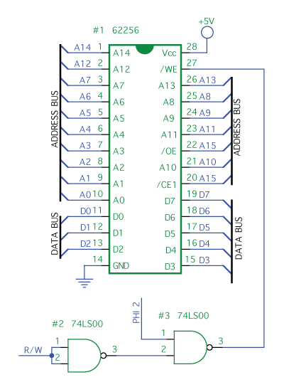 Figure 7.19 32 KB RAM Schematic |
Implementing the EPROM
If you want to use an erasable programmable read-only memory (EPROM) solely for the Monitor program, as the Apple I does, the circuit is straightforward. This design uses a 2716 EPROM, which is much bigger then we need, so address lines A8 through A10 are permanently tied low. This leaves us with 28, or 256, bytes of addressable space—exactly the number we need for the Monitor ROM range of $FF00 to $FFFF. Address lines A0 through A7 can be connected to the address bus, and the data lines can be connected to the data bus.
Output Enable, which is active-low, should be low whenever read is high; subsequently, /OE is connected to the R/W line through an inverter. Lastly, the chip should be enabled whenever the address is in the $FFxx range. Refer to the schematic in Figure 7.20.
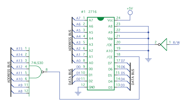
Figure 7.20 2716 EPROM Schematic
EPROM and EEPROM An EPROM is a programmable read-only memory (PROM) that can be erased under ultraviolet light. An electrically-erasable programmable read-only memory is an EPROM that can be erased with an electrical charge. Both EPROMs and EEPROMs can be read an unlimited number of times, but erasing and writing is typically limited to a few hundred thousand times. EPROM is pronounced ee-prom, and EEPROM is pronounced ee-ee-prom. |
Implementing the Expanded ROM
The Replica I uses an alternative chip for the ROM, a 28c64. It also uses a more complex method for chip enable. The EEPROM can be enabled for the entire range from $E000 to $FFFF. This can be conveniently done with a 74LS138 decoder. This same decoder can also be used to decode the addresses for our 6821 PIA, discussed in the next section; therefore, it is advantageous to become familiar with its use at this point.
Wiring the 74LS138
The 74LS138 is a one-of-eight decoder, giving us eight possible outputs. The EEPROM requires addresses $E000 through $FFFF. The 6821 PIA discussed later uses the $Dxxx range. Ranges $Axxx, $Bxxx, and $Cxxx aren't used, but since we have extra outputs, we can make them available for future projects. Table 7.3 shows the ranges expressed as hexadecimal and binary values.
| Hexadecimal | Binary |
| $Axxx | 1010 xxxx xxxx xxxxb |
| $Bxxx | 1011 xxxx xxxx xxxxb |
| $Cxxx | 1100 xxxx xxxx xxxxb |
| $Dxxx | 1101 xxxx xxxx xxxxb |
| $Exxx | 1110 xxxx xxxx xxxxb |
| $Fxxx | 1111 xxxx xxxx xxxxb |
The highest bit (A15) is 1 for all the ranges we're working with, so A15 can simply be used as an enable line (G1). Bits A12, A13, and A14 all vary, so they will be the input lines A, B, and C. For the range $Fxxx, ABC = 111b. 111b equals 7, making the output Y7 true. For $Exxx, ABC = 110b, which is 6 in binary, making Y6 true. The EEPROM should be enabled whenever Y6 or Y7 is true. Since /CE, /Y6, and /Y7 are all active-low, we should have an OR gate with an inverter at each input and output. Using DeMorgan's Laws, this is equivalent to an AND gate. Since this design already has a 7400 IC on board, a NAND followed by another NAND (to invert) is equivalent.
Wiring the 28c64
Since we're using this EEPROM as a simple ROM, Write Enable (/WE) is permanently tied high. The chip is only enabled when data is to be read from it, so it follows that /OE = /CE. The address lines go directly to the address bus and the data lines go directly to the data bus. A schematic of this is shown in Figure 7.21.
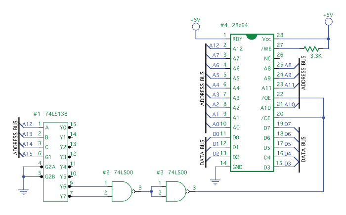
Figure 7.21 28c64 EEPROM Schematic
I/O with the 6821
The Motorola 6821 (Figure 7.22) is a peripheral interface adapter (PIA), which means that it's used for interfacing peripherals, such as keyboard and video, to the computer. The 6821 has two configurable eight-bit ports, PA and PB (for "port A" and "port B"), which can be used either for output or input. The Apple I uses PA for input from the keyboard and PB for output to the video circuit. The data is transferred to and from the computer via the data bus.
This section will provide a rather in-depth look at the operation of the 6821. If you plan to use the Apple I's standard interfaces for keyboard in and video out, this section might not interest you. If, on the other hand, you intend to substantially modify the Apple I circuit for some special purpose, or if you are interested in building your own microcomputer using the 6821, this information will be very helpful.
Each eight-bit port can be configured for either input or output. In fact, each bit direction in each port can be individually specified. When the Apple I is reset, the Monitor configures the 6821 to work with our circuit. On reset, both ports default to being inputs and the keyboard port is left untouched. The video port is set to output except for the highest bit, which is used as the "Data Available" line.
Figure 7.22 PIA 6821 Pinout
The Monitor uses the information in Table 7.4 for setting up the address lines. Changing the value of the bits CRA 2 and CRB 2 can alter which register lines that RS1 and RS0 address. The bits in Control Register A (CRA), including bit 2 (CRA 2), can be set when RS1 = 1 and RS2 = 0. First, set CRA 2 to 0. Next, make RS1 = 0 and RS0 = 0. This allows us to pass eight bits to the 6821 that will set the data direction for register A. Then, set RS1 high and RS0 low to access CRA and then set CRA 2 to 0. Now, when RS1 = 0 and RS0 = 0, Peripheral Register A will be accessed, whether for reading or writing, depending upon which data direction bits were set. The same technique applies to Peripheral Register B.
| RS1 | RS0 | Location Selection | ||
| CRA 2 | CRB 2 | |||
| 0 | 0 | 1 | X | Peripheral Register A |
| 0 | 0 | 0 | X | Data Direction Register A |
| 0 | 1 | X | X | Control Register A |
| 1 | 0 | X | 1 | Peripheral Register B |
| 1 | 0 | X | 0 | Data Direction Register B |
| 1 | 1 | X | X | Control Register B |
Take a look at Figure 7.23. The Register Select lines RS0 and RS1 are connected to the Address lines A0 and A1, respectively. The chip select line CS0 goes to A4. For the other chip select, CS2, we use the same 74LS138 as in the memory section to decode the high bits in the address, giving us everything in the $Dxxx range. This combination of decoding makes it possible for us to use the addresses seen in Table 7.5.
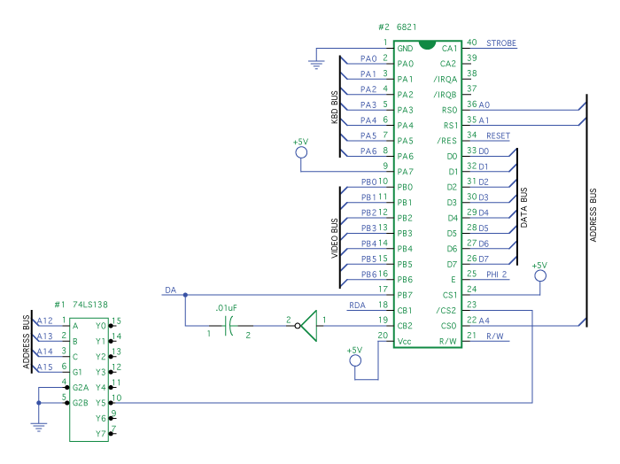
Figure 7.23 Control Registers A and B
| Mnemonic | Apple I Name | 6821 Name | Address | Description |
| DSP | Display Register | Peripheral Register B | $D012 | A character being sent to the display is held in this register until the video section is ready to take it. |
| DSPCR | Display Control Register | Control Register B | $D013 | Defines the behavior of the Display Register. |
| KBD | Keyboard Register | Peripheral Register A | $D010 | A character from the keyboard is held in this register until it is requested by the processor. |
| KBDCR | Keyboard Controller Register | Control Register A | $D011 | Defines the behavior of the Keyboard Register. |
When the circuit is reset, the DSP and KBD ports are in configuration mode (that is, bits CRA 2 and CRB 2 are low). This means that when we send data to DSP or KBD, it will go to the data direction register instead of the peripheral register. By sending $7F (that's 0111 1111b) to DSP, the lower seven bits are set to outputs and the highest bit is set to an input.
Next, the control registers (Figures 7.24 and 7.25) need to be configured. Both are configured in the same way, as shown in Figure 7.26.
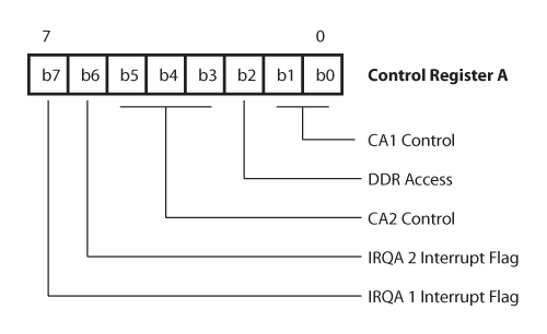
Figure 7.24 Keyboard Control Register
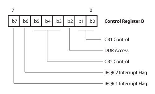
Figure 7.25 Display Control Register

Figure 7.26 Control Registers A and B
DDR Access
Note that b2, which is CRA 2 and CRB 2, is high. This changes the register selection from the data direction register to the peripheral register. Now, data sent to DSP and KBD will go to the peripheral registers, not to the data direction registers.
CA1 (CB1) Control
b0 enables interrupts on CA1 and CB1. CA1 is connected to the keyboard's strobe line. Whenever the keyboard sends a strobe signal, the 6821 loads the character on the KBD bus into its keyboard register. CB1 is used for the video circuit and is connected to RDA (Ready Data Accept). RDA comes from the video section and tells the 6821 that the video section is ready to receive a character.
b1 is high, which sets CA1 and CB1 to look for high-to-low transitions, as opposed to low-to-high transitions. This means that a change from 0 to 1 will cause an interrupt, whereas a change from 1 to 0 will not.
CA2 (CB2) Control
The keyboard's CA2 has no connection; consequently, these settings are only important for the video's CB2. b5 is high, which means CB2 is an output. b4 does nothing in this configuration. b3 is a flag which goes high when CB1, which is connected to the RDA line, goes high. The flag is cleared on the clock pulse (Phi 2 on pin E) after data is loaded into the display register.
IRA Interrupt Flags
IRQA and IRQB are not used.
Keyboard
When a pulse arrives on the strobe line, the character from the keyboard is loaded into the keyboard register and a flag is set in the keyboard control register. In the Apple I's memory map, the keyboard register is at $D010 and the keyboard control register is at $D011. The processor checks for the flag at $D011. When it sees it, the processor goes to $D010 and loads the character.
Video
The processor sends a character to the 6821, which then sends it out to the video section. The display register is at $D012. Before sending data, the processor checks bit 7 at memory location $D012. If this bit is high, it means the "Data Available" line is high, and the 6821 currently has data it is waiting to send to the video section. The processor waits until the bit goes low, indicating the 6821 has sent its data and is now ready to talk to the processor. The processor then sends its character to the display register, which is located at $D012 in the memory map. The 6821 loads this character into the display register and tells the video section that it has data available by setting DA (Data Available) high. When the video section is ready, it responds by setting RDA (Ready Data Accept) high. The 6821 sends the character to the video section and sets DA to low.
Keyboard Input
The Apple I uses a very simple ASCII keyboard (Figure 7.27). When a key is pressed, that character's seven-bit ASCII value is placed on the keyboard's data lines. A pulse on the strobe line indicates the data is ready. Many ASCII keyboards will also have a reset button. This button is connected to the processor's reset line. The rest of the signals, including data lines and strobe, go to the 6821. A schematic of this layout is shown in Figure 7.28.
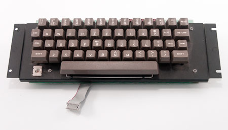
Figure 7.27 ASCII Keyboard
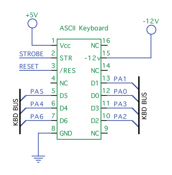
Figure 7.28 ASCII Keyboard Schematic
An ASCII keyboard is the simplest way to get data into an Apple I replica. Unfortunately, these keyboards are becoming very hard to find. The most reliable source is an Apple II+, but that computer is becoming a rarity in its own right. If you do borrow a II+ keyboard, treat the computer gently. The Apple II+ is a fun computer you'll want to keep around.
For those who can't find or don't want an ASCII keyboard, there is an alternative. Briel Computers has designed a PS/2 interface around an ATmega microcontroller (Figure 7.29). The PS/2 keyboard sends its scancodes to the microcontroller. The microcontroller converts them to ASCII and sends them to the 6821, using the strobe line to indicate when data is available.
You'll need an 8MHz crystal and two 18 pF capacitors to provide a clock for the microcontroller, and a PS/2 connector to plug your keyboard into. If you want the option of switching between a PS/2 keyboard and an ASCII keyboard, provide a jumper between the ATmega's reset pin and ground (as shown in Figure 7.29). Since Reset is active-low, jumpering it to ground will disable the ATmega by placing it permanently into reset mode, letting you use your ASCII keyboard without conflict.
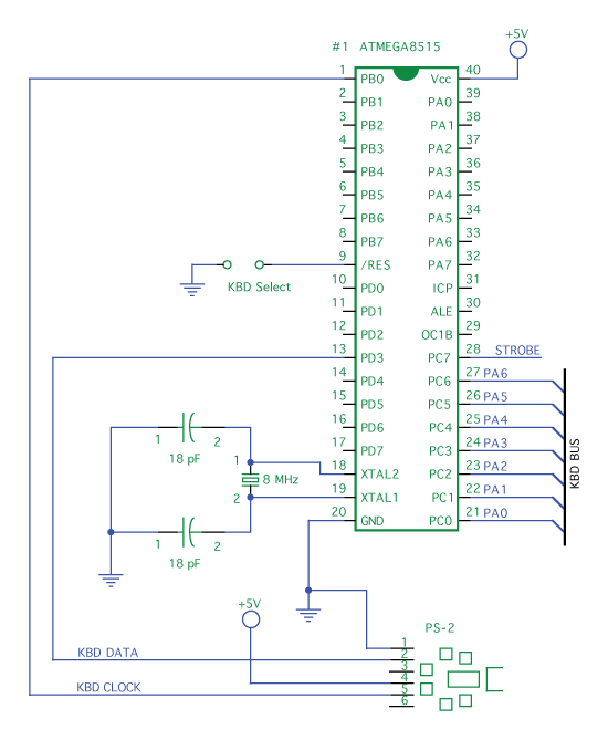
Figure 7.29 PS/2 Keyboard Schematic
Microcontrollers A microcontroller is a specialized microcomputer contained on a single chip. Microcontrollers are often used to control intelligent peripherals such as hard drives and are now common even in simple devices such as keyboards and mice. You'll find many Web sites and books devoted to the microcontroller hobby. |
Changes in the Replica 1 TE Briel Computers' newest version of the Replica, the Replica 1 TE, leaves the processor section unchanged, but significantly updates the video circuitry and keyboard interface. Instead of using an Atmel ATmega8 AVR and ATmega8515 for the video circuitry and keyboard interface, respectively, a Parallax Propeller microcontroller now handles both. The Propeller also provides a serial interface. The video section of the Propeller sends data to both the video port and serial interface, while the keyboard section listens for data from both the keyboard and serial interface. |
Video Output
The Apple I has very limited video capabilities. Most computers have video mapped to memory. On a black-and-white display, each pixel would be represented in memory by a single bit—1 for black and 0 for white. The Apple I's video section is text only. Instead of storing each individual pixel for a character, it stores the character's ASCII code. The video section has a ROM containing the pixel layouts for every character it supports. The layout table is referenced for each pixel of each character that is being displayed. This saves a tremendous amount of space, but at significant expense in versatility. Only the characters stored in that ROM can be displayed on screen. Thus, no bitmapped graphics can be displayed.
Even more limiting is the fact that once a character is sent to the display, it cannot be modified. It's there until you enter enough lines that it scrolls off the top of the screen, or until you manually clear the entire display. In this way, the function of the video is very similar to a typewriter or Teletype.
Why did Apple make these choices? At that time, memory—which would have allowed full graphics—was expensive. Instead, to save money, shift registers were used. When a character was sent to the video section, it was loaded into the shift register. As new characters appeared, it was slowly shifted through the register and then out. The Apple I's video section, which performed this shifting and then converted the signal into one readable video monitor, is far more complex than the processor section, which we've spent this chapter discussing. Understanding it also requires a decent knowledge of analog circuits, which is outside the scope of this book.
There are a couple of alternatives to a full-blown video section, such as hooking the output up to a Teletype, using a liquid crystal display (LCD) that accepts ASCII input, or setting up a serial connection to a PC. The option we're going to focus on uses a microcomputer design by Briel Computers to deliver output to a video monitor. This chip and a few TTL chips are equivalent to the original Apple I's video section.
You can see the circuit in Figure 7.30. At the center is the ATmega microcontroller, which is the heart of our video section. To the left of it is the clock circuitry. Depressing the Clear switch resets the microcontroller and clears the display. The 74LS74 is used as a clock divider, to cut the clock frequency down to about 7.1MHz. The 74LS166 is a shift register, which sends our data out to the display. Output goes to an ordinary composite monitor through an RCA jack (Figure 7.31) The diodes prevent any accidental signals the video monitor might generate from reaching and damaging the circuitry.
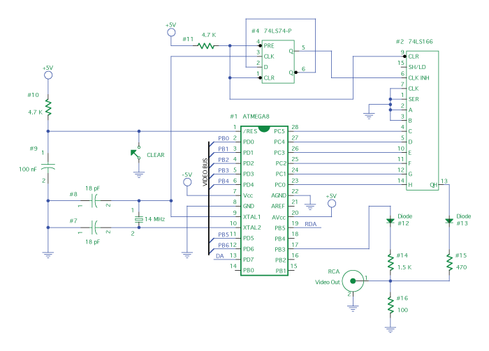
Figure 7.30 Briel Computers Replica I Video Section Schematic
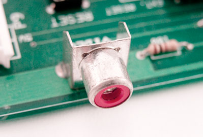
Figure 7.31 RCA Phono Jack
The electron beam in the video monitor's cathode ray tube (CRT) scans the display line by line. It starts in the upper-left corner and moves right. The display is black and white. When turned on, the electron beam creates a white pixel on the display, which indicates its current location. When turned off, that pixel remains black. A 0-volt signal turns the beam on to full power and creates a white pixel. A 3-volt signal turns it completely off. Anything in between produces a shade of gray.
The electron beam is constantly moving and our signal is constantly changing its voltage. If we wanted to send a line of alternating black and white pixels, we would alternate between 0 and 3 volts for every pixel. The beam then moves to the next line. When the entire display has been drawn, the electron beam moves back to the upper-left corner and begins drawing it over again. The entire process is so quick that the beam is redrawing the first pixels on the display before they even start to fade. Look at the CRT through the display of a digital camera and you'll be able to see a line moving down the screen as the display refreshes.
Summary
Though very simple relative to microcomputers today, there is nonetheless quite a bit to learn when studying the Apple I. In this chapter we've examined the processor, memory, and input/output circuitry. With this information, and perhaps some help from other members of the Apple I Owners Club on Applefritter, you can begin writing software and modifying the hardware design. Whatever your successes or failures, be sure to share what you learn with the rest of the Apple I community at www.applefritter.com/apple1.
| ← Previous | Contents | Next → |