
| Attachment | Size |
|---|---|
| 59.58 KB |
I just read UncleBernie's response here: https://www.applefritter.com/content/let-me-introduce-myself
So, I figured the timing was right to discuss the issue of SRAM write timing on an Apple II.
What I believe that UncleBernie is describing is a problem whereby if you synchronize the write with the fall of Phi2 that it is too late. The address and/or data is now corrupted, on the busses, and the data written will be bad. There is a similar problem, on Atari computers, due to the buffering of Phi2. I am also thinking the data bus corruption issue may be made worse because after Phi2 falls, the address and data busses are now used by the video subsystem so the additional hold time of the CPU is effectively eliminated.
I was looking into using SRAM and was thinking that it may be possible to use SRAM if the SRAM's write enable signal is high on read and low when the CPU R/W is low and /CAS is low. This would result in the SRAM write enable going high when /CAS goes high...which should result in the data being written before Phi2 falls and the busses are corrupted.
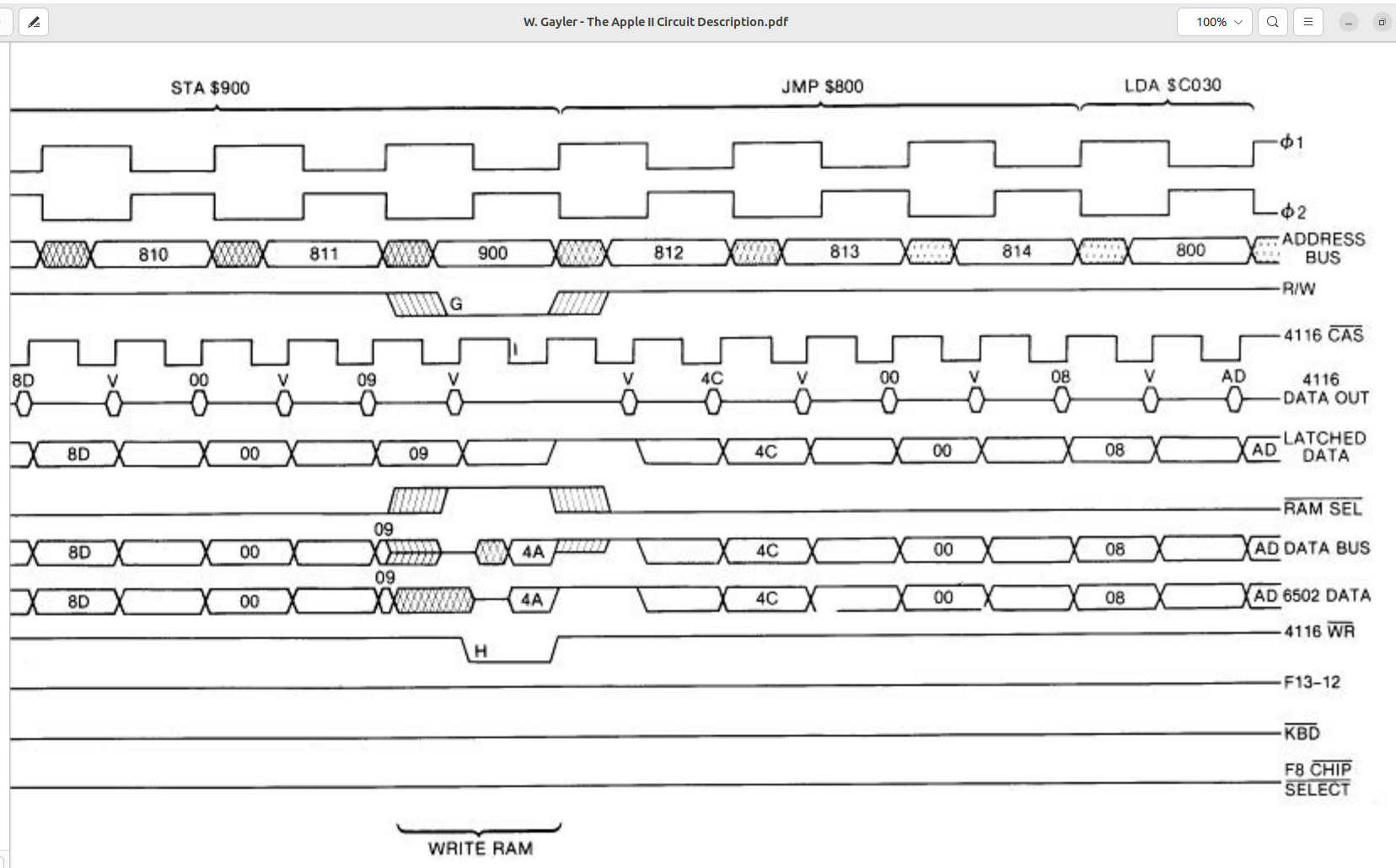
This chart shows why you wouldn't want to use Phi0 or Phi2 to synchronize the write timing:
While I didn't think about it, the soft switch latches should also be set using the same timing as writes to SRAM are set.
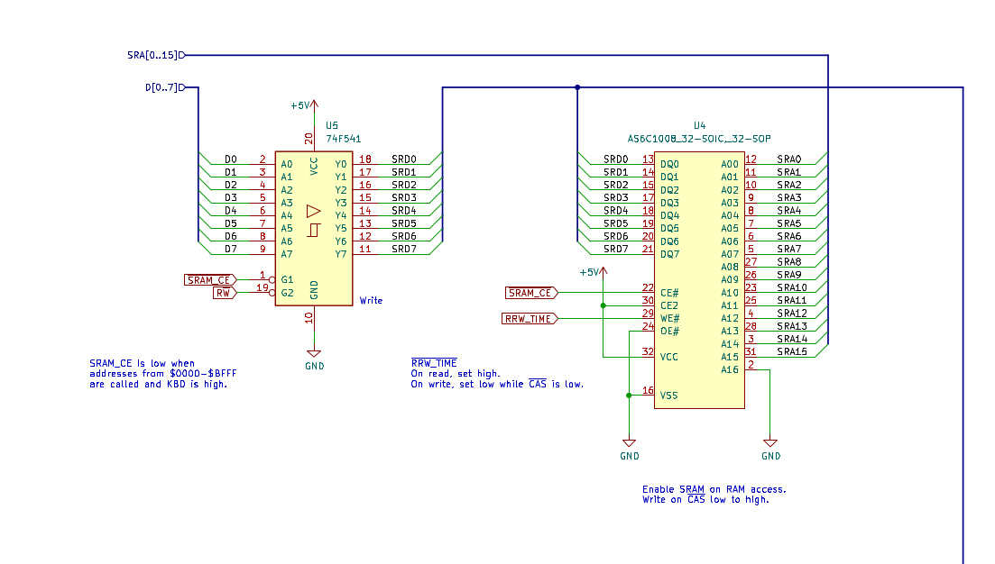
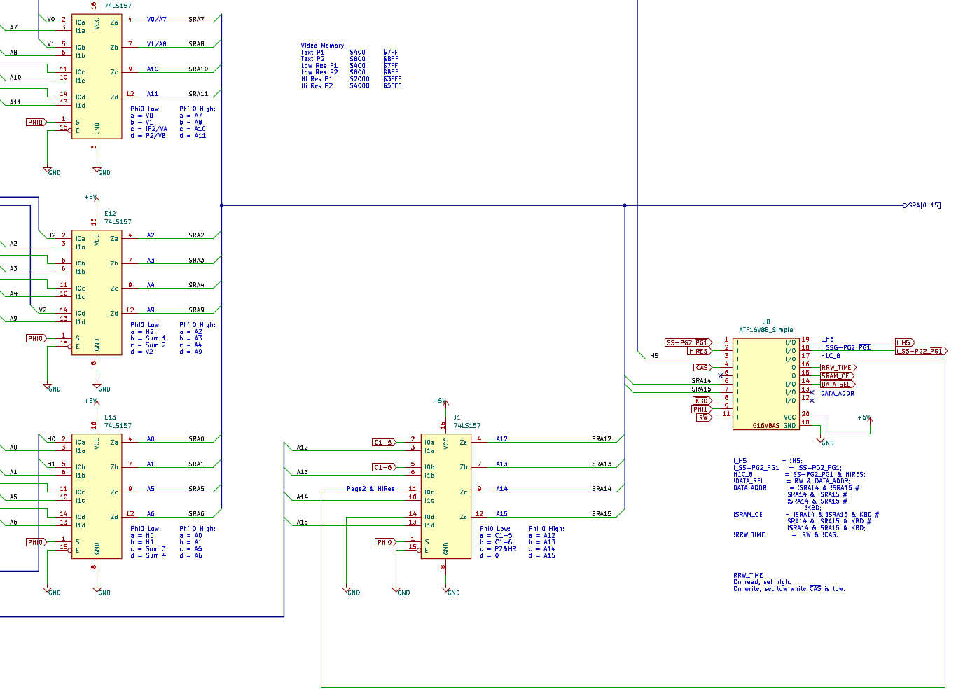
I was thinking it would be possible to use a PLD to build an apple II using SRAM like this:
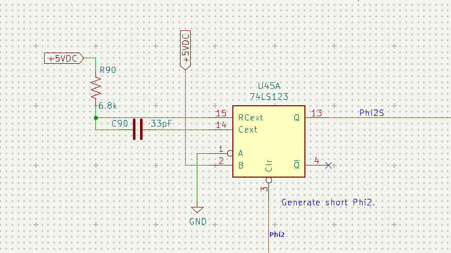
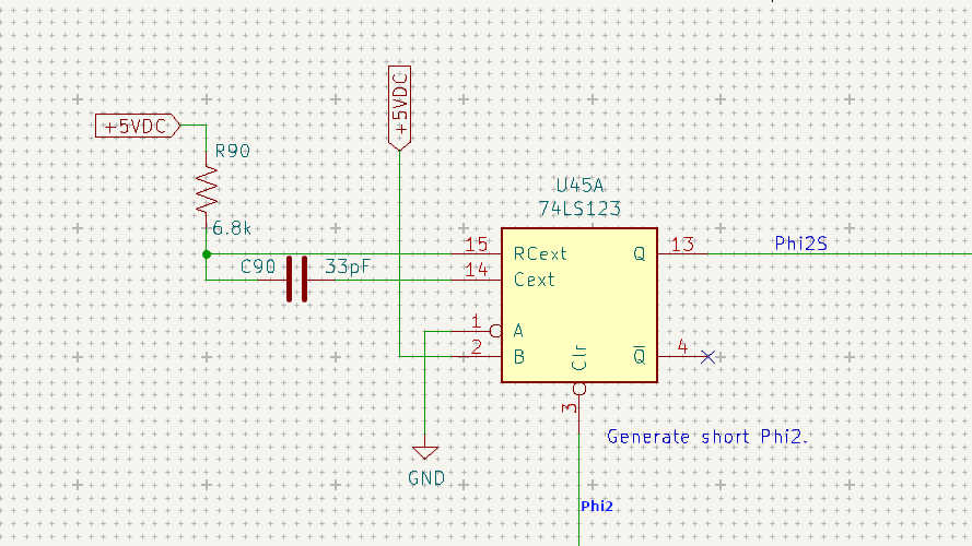
If using /CAS and RW for timing doesn't work, I think the next option would be to use a shortened Phi2 circuit like below and synchronize it with the write signal.
C90 and /or R90 may need some adjustment as this is used to time write signals on Atari PBI devices.
Thoughts?
I used 5156 or 6264 8K SRAM on 65C02 co-processor boards in four (4) Apple IIe slots that used the Apple IIe clocks and an AE TimeMaster card for interrupt cycling to control when the Apple IIe had R/W control of the address and data buses and these SRAMs worked just fine. Your project is using more modern SRAM's it appears.
In post #1, "reifsnyderb" wrote:
" There is a similar problem, on Atari computers, due to the buffering of Phi2 "
Uncle Bernie comments:
Actually, it's the same problem. Just that it gets worse when the PHI2 coming from the CPU is delayed even further, by adding buffers. Any gating logic / decoders also add such delay and at some point it doesn't work anymore.
You are right that shortening the write gate pulse to the RAMs is part of the fix.
This is what I did in 1987/88 with a famous Atari product of mine. The 1st generation of which failed at the customer all too often. The analysis of the problem was quick, after I paid the price of a new car for a brand new, 4 ch, 150 MHz oscilloscope. Fixing the problem was not so quick because from the Atari's parallel bus standpoint, shortening the write pulse entails "looking into the future". So I had a small injection locked oscillator on the 2nd generation of said product and a Signetics 82S105 FPLA for the revised logic. These 2nd generation products worked fine. Since then I'm allergic to that 6502 timing flaw. I think it was not incompetence of the 6502 designers - in Y1975 the typical SRAM or ROM was so pityfully slow that they did work despite of the flaw. And in Y1975 nobody may have expected that a NMOS 8-bit microprocessor still would be in production 12 years later.
But shortening the write gate pulse does not fix the issue with the crumbling addresses as such. This may affect the soft switches. And this is why the designers of the Apple II MMU and IOU custom ICs have moved the soft switch update to the last 14.31818 MHz clock cycle of the PHI2 phase (the "fake" one).
In my IOU/MMU substitute, I use no latches for the soft switches, but edge triggered D-Flipflops, which update the selected soft switch at the rising edge of the (fake) PHI2. This is a small deviation from the original IOU/MMU, but essentially is the same soft switch timing as the original, TTL-based Apple II had. Where the timing problem still is lurking, as Woz did use latches !
I'm not so sure whether this difference may affect Apple IIe software. I still have the problem with "Wings of Fury" crashing randomly after several hours of running in its demo mode. But I can't see any reason why the different soft switch timing could affect its operation. More investigations are necessary.
Running 6502 really fast
If you attempt to run a 6502 at much faster clock speeds than 1 MHz, you will find out that you will need much faster RAMs. I happen to have some CY7C185A-15 with a 15ns cycle time and a 10ns "Address Set-up to write end" time. On read cycles, the data is guaranteed to be stable for only 3ns after address changes. This is where the address change issue may strike, even at read cycles (how to guarantee the read data hold time of the 65SC02 ?). This requires very careful planning of the timing, and is the reason why I didn't try yet to bring all the extra stuff in the "CPU island" online. Theoretically, this fast RAM would allow running the WDC65SC02 at the system master clock speed of 14.31818 MHz. But timing calculations show that generating the control signals for the CY7C185 may be very, very tricky at that speed. I have planned for a 22V10-10 to do that (it has max 10ns propagation delay) but so far I see no way to implement the CPU island control logic as a fully synchronous state machine (having only the M14 clock). I may need an asynchronous state machine which would give me the equivalent clock speed (but with no clock being used) of 100 MHz, or even higher, as the 10ns selection of the 22V10 typically is switching faster than 10ns.
When everything progresses as planned, all the address, data, R/W signals outside of the CPU island will be sanitized to a point where anybody could connect anything to that sanitized bus, and it would work robustly, even if some TTL gate delays are added in the control signal paths. The CPU island controller would make sure that all setup and hold times of the 6502 and the memories would be observed under all conditions. For this reason I don't use normal bus drivers, as seen in the original Apple II and IIe design, but octal latches with tristate outputs. These can capture the address and write data coming from the 6502 to extend the hold time far into the next PHI1 cycle. But due to the video access cycle there, the data bus must be released earlier than expected. For read cycles, another octal latch captures the read data, and presents it to the 6502 as long as needed. Theoretically, this could be done by using "bit vapors" but I despise this technique, and it does not save IC package count, as an octal tristate data bus driver would be needed anyways. So why take risks ?
"Vaporlock" risks
Now, the evil technique of "bit vapors" has been named. The "vaporlock" programming technique used by many Apple II games is a concern, as it hinges on reading "bit vapors" left over from the previous screen byte fetch lingering on the data bus. I have plans to add yet another octal latch with tristate outputs to make the "bit vapors" more persistent, if that is necessary. The issue here is that with reduced IC count on the internal MD[7:0] data bus, and a more compact PCB layout, there is much less parasitic capacitance to "hold" the "bit vapors" until the end of the next PHI2 cycle, where the "vaporlock" routine would read them "out of thin air". That is, from a floating data bus. This is a very rotten technique. But it so happened that early Apple game programmers somehow discovered this foul trick and used it in their games, and unless it works, the game may hang forever waiting for signs of a vertical blank. The game "Drol", when running on the LinApple emulator under Linux, hangs in the 4th game screen (which is a cut scene, where the "kids" run to their "mom") due to a botched "vaporlock" implementation which does not work on that version of that emulator. So I'm well aware of the problem.
Other uses of "bit vapors"
Just as a side node, the designers of the National Semiconductors "IMP-16" chipset, which in 1973 or so was the first commercially available 16-bit microprocessor (on a set of five PMOS ICs) had the audacity to run the whole communication between these five ICs on "bit vapors". Which forced them to add a bunch of discrete capacitors on these internal signals once they found out that the idea to use dynamic storage nodes on the PCB was rotten. Within a full custom MOS IC, dynamic storage nodes work fine, until down to the 0.8um process node, where a multitude of issues affect it so badly that added design effort is needed to make it work, which is not worth it, as fully static storage nodes got small enough in area to use them throughout the IC. The NMOS 6502 uses lots of dynamic storage nodes, and would not have been feasable as a fully static design (die area would have gotten too large).
Historical "rear mirror view"
It's really fun to look back in time and see how the MOS design paradigms changed. In 1968 or so they had four phase dynamic PMOS logic, the 1974 Motorola 6800 already had two phase dynamic NMOS logic, the 1975 6502 had the same but added depletion load transistors, and in the 1980s dynamic logic died off and everything became static logic. Nowadays the big issue in digital IC design is the clock distribution system. Maybe we go back to 1970s design styles using multiphase clocks, but, of course, everything being static CMOS logic. Dynamic logic is dead, because the structures are so small now that the charges stored on dynamic nodes are too small to be used as a storage method. Any nearby signal lines could make them flip ... not good !
- Uncle Bernie
In post #2, LaserMaster wrote:
" I used 5156 or 6264 8K SRAM on 65C02 co-processor boards in four (4) Apple IIe slots that used the Apple IIe clocks and an AE TimeMaster card for interrupt cycling to control when the Apple IIe had R/W control of the address and data buses and these SRAMs worked just fine."
Uncle Bernie comments:
The CMOS 6502 is a completely new design and it is quite possible that they put some improvements in regarding the address and data hold times at the end of the PHI2 phase. CMOS also has steeper rise and fall times on its signals so the added timing "uncertainity zone" cause by the interaction of sloppy edges, ground bounce, and process variations of logical threshold levels is smaller. The downside of course is that the faster switching of typical polysilicon gate CMOS produces even fiercer current spikes on the power and ground rails. The only "benign" CMOS technology in this respect is the lame, early 1970s metal gate logic family CD4xxx. These still work when using plugboards with flight wires. 74HCTxx does not work in that environment. 74ACTxxx is even faster and should be avoided unless a good PCB design is used.
But I did not study the 65C02 yet. Some specimen are incoming, though.
Be assured that with the NMOS 6502, the problem is real. Just from simple pencil-on-paper calculations, it can be shown that it is all but impossible to design a NMOS 6502 system using the "official" memory and peripheral gating method based on PHI2 coming from the CPU itself, without violating address and data hold times all over the place. Unless, of course, you have magical TTL gates with a zero or even negative propagation delay.
The irony is that this false advice on how the PHI2 offered by the 6502 should be used was still in the "official" application notes from the various 6502 manufacturers even in Y1980 ! For instance, the "APPLICATIONS INFORMATION AN-2 / SY6500 Microprocessor Family" from Synertek, dated January 1980.
Anyone naively following their advice is set up to fall into that trap. The designers of the Atari 600XL/800XL did. This is why all the nice, planned and announced expansion hardware which intended to use the parallel bus connector on these machines was disappeared without a trace. They just could not make them work. But what can I say. I fell into that trap myself. But only once.
- Uncle Bernie
Uncle Bernie:
Thanks for the detailed reply. What Atari PBI product did you work on?
I wasn't thinking, initially, of running the processor faster than 1 MHz. But it is a thought, of mine, that it might be relatively easy to at least go to 2 or 4 MHz at some point. The SRAM is 55ns, so I don't want to push it. Also, the transition times of the various chips need to be checked. But 1 MHz is the first goal, of course.
I am thinking about adding the capability of connecting a 74LS123, as I suggested, in the event that timing via /CAS and RW is still too late. I don't think that would be a big deal because I think it would be nice to have a breadboard on the PCB anyhow.
I am glad you mentioned the vapor lock and bit vapor issues. I didn't realize what was going on until I read your reponse several times and also looked it up online. (I am very new to Apple computers.) In retrospect, I found it odd that nobody made a hack to add some sort of HBLANK and VBLANK signals. (Atari's could just be setup to utilize an NMI and life was good.) On the note of the bit vapor issues and capacitance, maybe it would be a good idea to add a low value capacitor to each of the data lines? Maybe something like a 1nf capacitor would be enough? 1nf might be small enough to keep the residual data without invoking too much of a delay when the data bus is set. I think you are referring to something similar being done on the "IMP-16"?
Thanks!
Brian
Uncle Bernie Writes:
"Anyone naively following their advice is set up to fall into that trap. The designers of the Atari 600XL/800XL did. This is why all the nice, planned and announced expansion hardware which intended to use the parallel bus connector on these machines was disappeared without a trace. They just could not make them work. But what can I say. I fell into that trap myself. But only once."
It's funny you mentioned this. I've got copies of Atari's 1090XL card schematics and their 1064 memory upgrade. What is striking is that Atari supplies Phi2 at the PBI. Then, Atari's cards don't use Phi2 directly, and, instead, have their own delay lines for timing. Because of this, I came to the conclusion that Atari engineers figured out that Phi2 wouldn't work as planned. That is also why people, over at the AtariAge forums, mentioned using the 74LS123 circuit I posted for creating a shortened Phi2 signal to still use Phi2 for timing. It works great on the cards I designed.
Just to mention Apple themselves used SRAM back then in some of their peripheral cards, for example the 6164 in SCSI card's buffer and the 6116 in the 80-column text card for the AUX slot (and in Liron 3.5" drive PCB but the this is a different story).
You wrote: "What Atari PBI product did you work on ?"
I had my own company at the time. True Atari aficionados know this product. Modernized and more capable versions (more RAM, more FLASH on board) were still being produced in small batches every few years, at least until Y2016. I made the design and source code "open source" maybe 20 years or so ago. And some capable enthusiasts took this information and designed the new generations. And then produced them. Small batches, not really commercially viable, but still, which product for the Atari 8-bit is still in "production" after 30 years ?
You wrote: "I am thinking about adding the capability of connecting a 74LS123 ..."
A valid approach to shorten the write cycles. But be aware that you need to measure each and every 74LS123 and find a resistor / capacitor combo which produces the correct timing delay. I had to do that with every 74123 that went into my famous Apple-1 kits. Very tedious. In the electronics industry, use of such oneshots was discouraged due to the extra costs for the trim adjustments when more exact timing was required.
You wrote: "In retrospect, I found it odd that nobody made a hack to add some sort of HBLANK and VBLANK signals."
The Apple II never needs synchronization of the running program with the electron beam in the CRT. The STA WSYNC of the Atari 8-bit was necessary to be able to "race the beam", a carryover from the Atari VCS. But what the Apple II really needed was to find out where the Vblank period is. At that point, the PAGE soft switch could be changed, so the next field on the CRT screen would be generated from the other graphics page. This is very important to get smooth animation. See the game "BANDITS" for what happens when this is not done. In the start screen, a small car or van drives away from the spaceship, and it is jerking / wobbling / shape shifting in the worst possible way. This is because the human eye can still "see" when shapes on screen are changed while they are being drawn by the electron beam. The Apple IIe and IIc have added hardware to read the VBL status. So a game which can only run on these machines anyways (earlier Apple II had no double hires) would not need vaporlock tricks. Which does not mean that the game programmers didn't use them on the Apple IIc and IIe.
You wrote: " Maybe something like a 1nf capacitor would be enough ? "
Just as an example, to change the voltage on a 1 nF capacitor by 3 Volts within 100ns, you need a driver able to sink or source 30mA. This requires some fairly beefy drivers. Not out of reach, but be aware that NMOS drivers to "H" level are notoriously weak. I wouldn't do that. There are better ways to design bus holders. But it's not easy. They must be able to sink or source the input currents of the various TTLs attached to the bus. This problem goes away when using 74HCTxxx. No static input currents to drive on those. But 74HCT is already so fast that it makes fierce current spikes on the power and ground rails. Very good PCB layout and proper design of the power supply bypass circuits is required. This can get tricky if the parasitic inductors of the traces, combined with the bypass capacitors, produce high Q resonant tank circuits. If any periodic signal in the system gets close enough to that resonant frequency, all hell breaks loose. All of this ain't "electronics design 101" anymore. It's a topic for the higher semesters ...
BTW, IIRC, the DEC LSI-11 also may have had signal holding capacitors on some internal signals running between the custom LSIs (which were not designed by DEC). It's just too late at night to try find a LSI 11 CPU board in my basement to verify that. I also seem to remember that the first DRAM was built in the late 1940s or in the 1950s, and it was a drum with many contacts on the circumfence, one contact per bit cell. The bit cells were capacitors mounted within the drum. A set of static brushes contacted one set of bits ("word") at the time. Access time was dictated by the rotation speed of the drum. This contraption also needed bit read amplifiers (vacuum tubes) which also did the refresh. So when decades later the DRAM ICs came up, the basic idea for DRAM (one capacitor per bit cell) could not be patented anymore.
Uncle Bernie
LOL, and what would they say about working out new designs for it half a centruy later in 2024?!?!?!
Considering how many of those guys like Chuck Peddle have left us, who knows... Not sure how many of them who were or are still around the past few years were really that aware of the retro scene. It's not really that big, most people I talk to have no idea it exists. And I'm currently working at a majpr semiconductor company.
Since you guys are getting into the weeds here, it should be noted that there were several cards that used SRAM BITD. Here is a Legend card that had 18K of battery-backed SRAM (16K Language Card + 2K IOSTB space). And as UncleBernie pointed out in his earlier post, it is notable the Apple II's DO NOT USE the 6502 generated PHI2 signal (they just use an inverted PHI0).
IMG_5255.jpg
In post #9, "jeff d" wrote:
"LOL, and what would they say about working out new designs for it half a century later in 2024 ?!?!?!"
In post #10, "softwarejanitor" wrote:
"Not sure how many of them ... were really that aware of the retro scene. It's not really that big, most people I talk to have no idea it exists. And I'm currently working at a major semiconductor company."
Uncle Bernie comments:
Losing Chuck Peddle was a big blow to my own research on the Apple-1. I'd really needed to find out about the Garage episode with Woz. This is a big piece in the Apple-1 history puzzle.
Bill Mensch is still around ! And so is his 6502 - it's maybe the only general purpose 8-bit microprocessor of the 1970s still in production after half a century. The basic design has morphed towards more modern techniques, however, it's now all RTL (IIRC, Verilog). It's still successful on the marketplace. It goes mainly into embedded systems where an ARM core would be overkill and a 8051 core too weak (the 8051 is no true 8-bit processor, and the PICs are not "general purpose" due to their architecture optimized as I/O processors, and they sell no RTL cores, AFAIK).
As for the retro computing scene, my take is that it consists mainly of older guys who were kids or teenagers when the first homecomputers (Apple II, TRS-80, Commodore PET) came out in 1977. The "trailing edge" of this scene are those who are slightly younger and had Atari 8-bit computers, Commodore C-64, and the like.
Most curious and smart people I know have that gut feeling to have lost something of their youth when the homecomputers went the way of the dinosaur and now, many are retired and engage in "retro" computing activities revolving around these homecomputers, to bring back part of their lost youth. So it's essentially the same phenomenon as with vintage car collectors, or vacuum tube radio collectors, etc.
People working in semiconductor companies typically have no time for hobbies. So they are not representative for the general retro computing scene. I did not touch any of my computer collection during that phase of my life. As fascinating full custom analog / mixed signal IC design is, it's a job that fully sucks you in, like a black hole. The only escape is retirement.
My mission is a bit different. There is a selfish motive (keeping my braincells working) but also the desire to create a "living document" explaining and preserving the technology of the time. I had the privilege, as a student of electrical engineering, to have designed one of the last two phase clocked, NMOS depletion load, full custom ICs the university ever did. This was my Master's Thesis. Truly "trailing edge" process technology, but they had the credits towards one last wafer made in a wafer fab run by students of another university. And they didn't want to let this opportunity go to waste ! And what really mattered was the revolutionary architecture of this systolic array processor. So I had my chance to work with NMOS (L = 3.5 um) and learn the tricks of the trade. This is why I can fluently read the original 6502 schematics (and that skill also helped me with understanding the MMU). I'd love to apply that skill towards the Atari custom chips, too, but alas, high quality (readable) transistor level schematics of those were never found despite of all my searches on the web. The ones that exist are so badly scanned that it's too much guesswork left over to waste my time on that. Otherwise I could make accurate substitutes of these custom ICs within a few weeks.
Working with the Apple II architecture is more viable, as it is documented very well. I'm still looking for the IWM spec as written by Woz himself (if that mythical paper ever existed). Those IWM documents I could find on the web don't tell much about the extra functions over the Disk II controller. I have found the IWM patent but I think its obfuscated in some ways to avoid or distort some details probably found in the real silicon. So, alas, I can't have an accurate Apple IIc mode in my Replica 2e .... yet. The quest continues ! And for me, is a lot of fun !
- Uncle Bernie
In post #11, jeffmazur wrote:
" And as UncleBernie pointed out in his earlier post, it is notable the Apple II's DO NOT USE the 6502 generated PHI2 signal (they just use an inverted PHI0) ".
Uncle Bernie comments:
The Apple II slot bus only has the "fake" PHI1, PHI2 produced by a synchronous state machine on the motherboard. Except that they call the fake PHI2 "PHI0" --- which in 6502 canon is the clock input of the 6502 itself, but they did not use it as such, as they added a TTL gate for the clock stretching during DMA operations. This TTL gate brings a little bit more delay which is good for writes, but bad for reads. The PHI1, PHI2 signals offered by the 6502 are ignored.
If the fake PHI1, PHI2 signals are used to gate off the output enable (or chip select) of memories, the tristate drivers of the memory may turn off before the actual PHI2 phase of the 6502 is over. How do they guarantee the 6502 read data hold time (Thr in the dataheet) of 10ns ? Well, any gate delays between the origin of the PHI0 signal to that output enable (or chip select) pin make the turn-off delay longer, and this helps towards data hold time.
But as we have learned with "vaporlock", even "bit vapors" can linger on the data bus for a while, and the 6502 will happily accept these "bit vapors" as the read data, too.
So in the greater scheme of things, the Apple II slot bus architecture with the fake PHI1, PHI2 (aka PHI0) takes a lot of the 6502 timing problem out. It is quite robust. Had they used the PHI1, PHI2 signals offered by the 6502 for the slot bus, then there would have been lots of problems with making slot cards work. This is where other manufacturers of 6502 based computers shot themselves in the foot.
The discussion of this timing problem is not "getting into the woods" but is necessary and certainy helpful for anyone who ventures into designing a 6502 based system and NOT blindly copying Woz' "wrong" way of making fake PHI1, PHI2 signals. "Wrong" way works better ;-)
In hindsight, I think this problem came about because the 6502 was designed to be a fast processor despite using a slower master clock which defined the CPU cycles 1:1 --- compare that to the 8080, for instance. The 8080 has a much cleaner bus interface but to do that they had to use a much faster clock which MOS could not handle, so the 8080 is surrounded by the 8224 timing generator and 8228 system controller, both made with TTL. This drives systems costs up. The Motorola 6800 used a NMOS process technology that was unable to generate the two phase clock on chip, so they needed the external clock drivers. These clock must be non-overlap, beyond many designers of the time, and so clever people made a hybrid module to generate the nonoverlap 6800 clocks, in a metal can. Which cost, IIRC, ~$50. But what the 6800 did better was the "VMA" signal for "valid memory address", which gated all the peripherals like the 6820, and the memories. This signal was dropped on the 6502. And I have a hunch that Chuck Peddle only got so furious at Woz (if the story is true at all and the garage meeting really happend) because he (Chuck) suddenly realized that his 6502 system architecture had a timing flaw,which he, Chuck, did not see, and Woz had seen it, and found a way to design around it. Clash of egos ! Would have been an interesting story to confirm if it really did happen.
- Uncle Bernie
Not written by Woz (actually Wendell Sander created the IWM), but a reproduction of the IWM has been done by Plamen of a2heaven. In case you haven't seen this .
In post #11, jeffmazur wrote:
" ... a reproduction of the IWM has been done by Plamen of a2heaven."
Uncle Bernie answers:
I have followed his Liron project for a while and I have the Verilog code for the IWM block he uses in it, which he posted on github. Had no time yet to compare his code to the IWM patent. I always try to get at original sources / original documentation. Plamen mentioned something about a IWM description by Woz he found in "dark corners of the web". Hmm. Would like to see that. All I found in terms of IWM documentation was stripped down to a point it's useless to make a substitute of the IWM. (Of course, they did that on purpose). The best info I found was some 68000 source code using the "other" mode of the IWM. I can read 68000 code but this does not help much to reconstruct a 100% accurate spec for the IWM.
- Uncle Bernie
For completeness, it should be noted that back in late 1978 EDN magazine presented a series on Project INDECOMP which was a system built upon the Apple II. Early on, they ran into issues designing a serial card to work in the Apple and this was traced to the unconventional PHI signals. This difficulty was chronicled in "real time" over several months of the series. Looked for a link to this article but couldn't find one.
In post #16, "jeffmazur" wrote"
" Early on, they ran into issues designing a serial card to work in the Apple and this was traced to the unconventional PHI signals. "
Uncle Bernie comments:
They should have looked into the original "Apple II Reference Manual" for the proper timing. With the "fake" PHI1, PHI2 (aka "PHI0", but I hate to use that here on Applefritter, where the font does not discern between zero and "o") it is much easier to design a robustly working slot card compared to the situation if Woz had used the PHI1, PHI2 offered by the 6502.
There is one important difference other than timing, and this is that 6502 signals are guaranteed to have no overlap of the "H" period. The "fake" ones don't have that feature. And if the "fake ones" enter certain combinatorial functions at the same time, there may be hazards, and if these hazard infested signals then are used to clock things, these things won't work.
It's always important to keep these effects in mind when designing stuff for the Apple II. Note that certain combinatorial functions between PHI2 aka PHI0 and Q3 on the slot bus also are subject to hazards / critical races. Some of the timing related circuits seen in Jim Sather's book on the Apple IIe won't work in the real world, or only work when the moon phase is right, and the trash can has been emptied, but as a description for the inner workings of the IOU/MMU these simplified schematics are OK.
The whole topic is not as easy as it looks superficially. Go down that rabbit hole and be surprised !
- Uncle Bernie