
| Attachment | Size |
|---|---|
 Capture d’écran 2026-08-26 à 23.25.23.png Capture d’écran 2026-08-26 à 23.25.23.png | 182.42 KB |
| IMG_5271.jpeg | 1.83 MB |
 SRAMTEST#06E000 SRAMTEST#06E000 | 326 bytes |
Today I got my CFFA1 from ReactiveMicro, many thanks to him!
I have unfortunately a problem while using it:
my Apple 1 replica corrupts data loaded through the CFFA1, but only above $1000. Text in my programs comes out garbled, and the garbling moves from one load to the next. The files themselves are fine — they run correctly under CFFA1 emulation (Honeycrisp)
Setup: replica board, Uncle Bernie reliability mods under the board, CFFA1 v1.0 RevD, firmware 1.1, in the onboard slot. No expansion board, no ACI. A–T jumper installed. S1: 2 OFF, 4 OFF, 5 ON, 6 ON. Motherboard RAM at $0000–$0FFF and $E000–$EFFF.
How I measured it. Rather than trusting what I see on screen, I load a file with L, then write it straight back with W two or three times without reloading, then compare checksums on a modern machine.
What I found:
Same file (2625 bytes), three consecutive writes each time:
- loaded at $E000 — three identical files
- loaded at $0300 — identical files
- loaded at $2000 — files differ
With a 14 KB program at $0300, errors pile up across successive writes without reloading: 13, then 18, then 21 bytes. Corrupted bytes never recover. Everything below $1000 is always clean.
Leaving the machine idle for 20 minutes adds nothing, and the prefix stored in $8000–$8FFF survives. So retention is fine — it only goes wrong during bus activity.
Two more things that may mean something to someone: across three independent runs and 60+ corrupted bytes, every faulty address has A2, A3, A4, A8, A9 and A10 high at the same time. And the value written over the original byte is $44 in most cases, whatever the original byte was.
MEMORYTEST won't run here either — it returns to the prompt immediately with no PASS. Since it loads through the same path,
Has anyone seen this pattern? I'd particularly like to know whether marginal motherboard DRAM can corrupt transfers into a card's SRAM without failing its own memory tests. I muss say that I'm a bit puzzled...
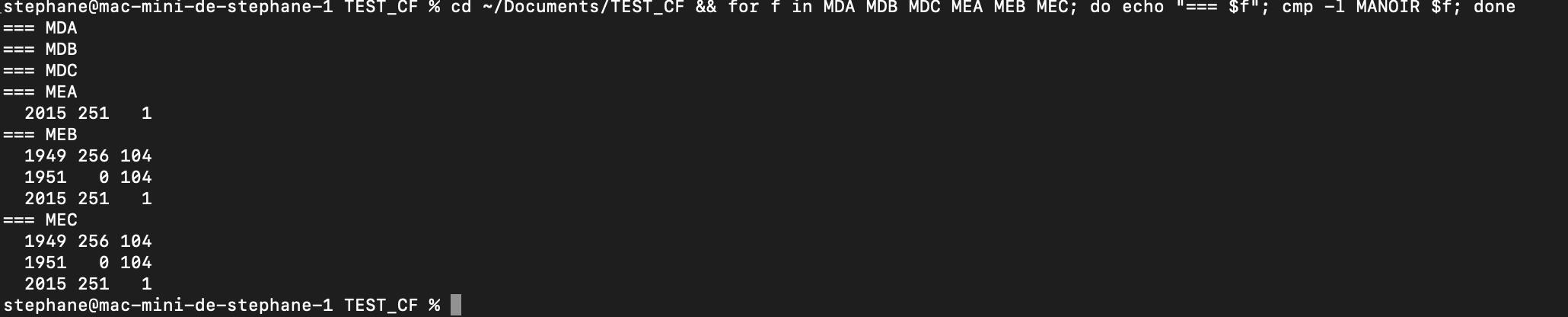
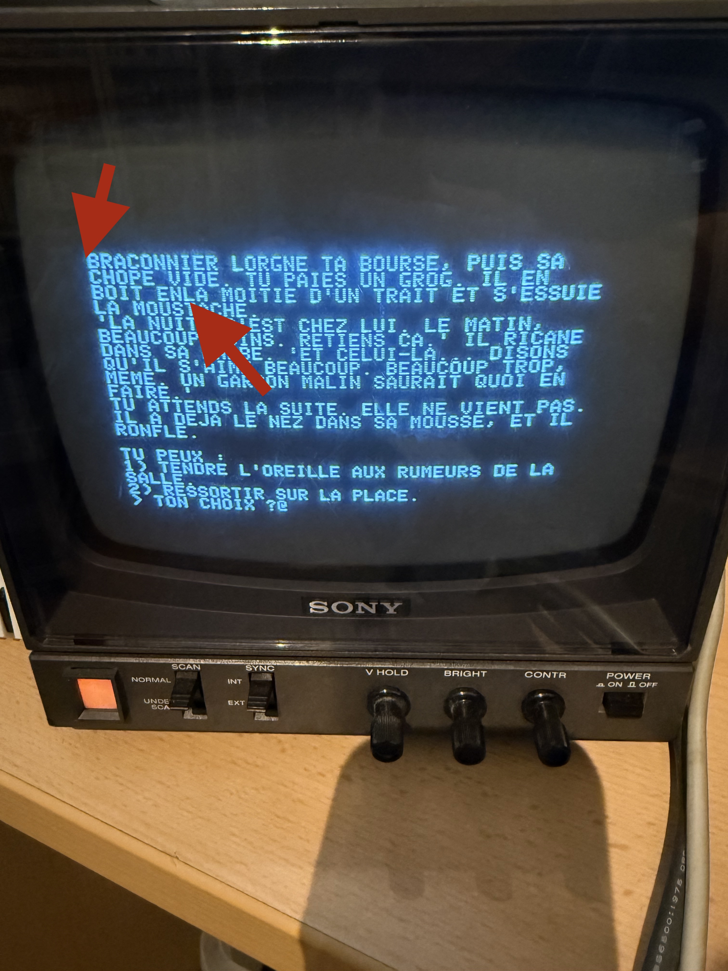
I join a cmp comparaison that show the differences between two saves with W and a screen of my game (in french) where we see that the text is messed up or characters (le before braconnier) is missing.
Thanks for your help!
UPDATE:
he CF card is not involved at all.
I asked Claude to write a small 6502 test program that runs from $E000 (motherboard DRAM, which is clean here). It fills the CFFA1 SRAM with a known pattern, then repeatedly re-reads it and counts mismatches. It has two entry points: one that also triggers CF block reads between passes, and one that does nothing but read the pattern back.
Both behave the same. Around 50 corrupted bytes after 8–9 passes, with or without any CF activity.
So the corruption happens on plain 6502 reads and writes to $1000–$7FFF. No file loading, no firmware calls, no block driver, no CF card access. The faulty addresses are the same ones every run, and they all still satisfy (address AND $071C) = $071C.
I think i can resume my actual problem thanks to the Memorytest programm from Mike this way:
I'm getting memory errors in the card's extended RAM. My own programs load into $1000–$7FFF and come out with corrupted text — a few wrong bytes each time, in different places on each load. The files themselves are fine.
To check this, I ran Mike Willegal's standard Apple-1 memory test on $1000–$7FFF. It stops immediately and drops back to the monitor prompt, which is what it does when it detects an error: test 0, address $275C, expected $00, read $28.
I then swapped the CFFA1 for the P-LAB SD card, which provides RAM in the same range through the same slot, and the same test keeps passing without errors.
Attached both pics: memory test running fine on the P-LAB card, and failing on the CFFA1.
I'm wondering whether the memory chip could be defective, or if something else might explain this? Have you seen this before?
IMG_5293.jpeg
IMG_5292.jpeg
I add a pic of the implementation of the reliability mod @UncleBernie: May I ask you what you think about my memory problem? I think that you are the most knowledgeable person in this area :-)
Thanks for your help!
IMG_6879.jpeg
and my jumper configuration, in case I didn't understood something obvious:
IMG_5286.jpeg
IMG_5287.jpeg
IMG_9691.png
Check your 6 resistor fix layout. Picture above for reference.I'm running the CFFA1 and no problems. Also do you have Uncle Bernie's PROMs? If so try the pin 14 DRAM program he made.
It could also be a problem with the timing resistor at B3 by keyboard connection? Touchy variable... But your 6 resistor fix is key. I've built 6 of these and without, none worked correctly.
IMG_9692.jpeg
Ok, I check this right away.
Do I understand right: none of your Apple 1 worked with the CFFA1 correctly without the resitor mod? Whas was the symptom?
I'm not sure about the ROM, I didn't assembled the machine myself. How can I tell what ROM I have?
Nice collection by the way :-)
I just took a look, and ther is one difference: the array of 3 resistors to the left aren't connected to the same place (left your pic, right mine). But mine is like what Uncle Bernie's mode describe. Can you elaborate on this modification, what is the difference between your implementation and mine, and will it help with the CFFA1 ?
dtc.png
Ha, and here is mine!
Capture d’écran 2026-08-28 à 21.01.47.png
Capture d’écran 2026-08-28 à 21.01.47.jpg
IMG_5098.jpeg
Thanks :-)
IMG_9693.png
Ok. so if I understand good, this is for ringing in the dram that is on the motherboard. But my dram on the motherboard pass the test, my problem is really that the ram exposed by the CFFA1 seems corrupted. You said that none of your machine worked well before the mode, it is regarding the onboard memory, or do you mean that none of your machine could operate the CFFA1 without the reliability mode like you did? If yes, what was your symptoms on the CFFA1 ? same than me, memory corrupted?
Thanks
Most of the builds had DRAM issues and especially problems when the ACI was installed without the 6 resistor fix. If you haven't, read and review, Uncle Bernie's fantastic manual! I bet your problem is with the 3 resistors going to Dram W6 instead of the 8T97 chip?? Move resistors to there as pictured and I bet your problem is solved?
ok, yes it's easy to do, I give a try.
Can you elaborage about your constatations with the CFFA1? Your feed-back is precious to me, as I don't find many testimonials online. When you experienced problems, was it with the CFFA1 itself and if yes, did you saw corrupted ram on the CFFA1 too?
There are not so much software that use more than 8k, therefore, someone using only programms that it in 8k won't see the problem.
Did you try to run the memory test from Mike on your CFFA1?
I used this and got errors, I would be really interested into your result, just to rull out that I'm not missunderstanding how the test is supposed to work:
here is the command I used:
L → MEMORYTEST → Enter(accep $0280)
Q
0: 00 10 00 80
280R
Thanks for your help!
I report when I tested the modification you advised me.
I have had absolutely no problems with the CFFA1 card. Wonderful device!! I worked out problems with ACI's before using the CFFA.
Could you share the PDF, or a link to it? I couldn't find it anywhere online. Thanks!
I will do the modification today and will report.
OK, I did the modification like you pointed out: saddly, there is no modification on the CFFA1 side: it still corrupt everythings that land in his 28k RAM and the memorytest still fail immediatly.
Then I launchend the Madhamer test to be sure, and the test pass for one hour in boths UncleBernie's mod configuration (Like it was and as you showed me). No error at all.
I'm really guessing now that the problem is on the sram of the CFFA1 itself, as I see no mechanism that can explain why a program loaded from the Apple 1 in extended ram could be corrupted if there is no ringing on the memory bus. But I hope that maybe @UncleBernie give his insight and maybe point me toward something I forgot or missunderstood!
Can you run the ram test on the CFFA1 like I did, just to confirm that it should work on a working sytem?
L → MEMORYTEST → Enter(accep $0280)
Q
0: 00 10 00 80
280R
IMG_5338.jpeg
I'm wondering something:
If r28 value is impacting the ACI board, maybe it's impacting the communication with the CFFA1 too?
In post #16, "guibrush" wrote:
" Then I launchend the Madhamer test to be sure, and the test pass for one hour in boths UncleBernie's mod configuration (Like it was and as you showed me). No error at all. "
Uncle Bernie comments:
"madhammer" is a specialized memory test I wrote to test the success of the six 390 Ohm damping resistors added with the "reliability mods". It uses an address pattern which according to my experiments had the worst ringing / crosstalk issue in the multiplexed address lines for the on-motherboard DRAM. By no means it is a complete memory test. It never was meant to replace the "diagnostics page" in the A-1, A-2 PROMs which came with my IC kits.
As the address multiplexers never chop up the addresses when neither one of the two DRAM banks on the Apple-1 motherboard is accessed, they can't compromise the SRAM addresses the CFFA card "sees".
I've never looked into the CFFA schematics and I don't have a CFFA, so I can't help any further. But you can look for yourself which signals gate the SRAM of the CFFA, and then (if you have a fast enough oscilloscope, 150 MHz BW and 10ns/div timebase is enough) compare these to the PHI2 signal on pin #39 of the 6502, which the Apple-1 (and the Apple II) does not use. Take a measurement from the falling edge of this "real" PHI2 to the gate off time of the SRAM write cycles on the CFFA and tell us the value.
It has been my experience that the NMOS 6502 bus timing concept, while it was fine in the 1970s, has some fatal flaws which manifest when using much faster RAMs which appeared in the mid 1980s or later. These fast SRAMs, if not gated off "soon enough" after the "real" PHI2 falls, can "see" the crumbling addresses coming from that, which in write cycles may corrupt their contents all over the place.
Back in the 1980s, I had to redesign one of my products due to this ill effect any NMOS 6502 has. The product used a 6116 SRAM. The remedy was to gate off the /WE earlier than the PHI2 falling edge. Which involves a "magic circuit" which can look into the future ... an injection locked oscillator clocking a fast state machine which self-synchronizes to the 6502 bus cycles. This made the problem go away.
The larger and more modern SRAMs used by the CFFA are much, much faster than this 1980s era 6116 and I don't think they would work with the Apple-1 unless such a solution to terminate the write cycles earlier is present. Which I can't tell without the CFFA schematic. (Yeah, I'm too lazy to even look for it on the internet ...)
Note that I'm not claiming that your CFFA suffers from this ill effect, but it is probable cause. Another possible cause is a defective SRAM which a few bad bit cells or a defective address decoder. Which would cause memory errors even if the above mentioned timing fix is present.
- Uncle Bernie
Thanks — I wasn't clear enough, sorry: I was using MadHammer for what you designed it: to confirm that the reliability mod is correctly implemented on my board. One hour, no errors, in both resistor placements — the original one and the corrected one Zero dB pointed me to. So the six damping resistors are doing their job if I get it right :-)
I tried to compil a small 6502 test programs to characterise the CFFA1 failure more precisely. Three results may interest you:
The corruption is entirely confined to addresses where A2, A3, A4, A8, A9 and A10 are all high — 512 addresses out of the 32 KB range. Over 400 KB of read-back across many runs, not one byte outside that set has ever been wrong. The failing addresses change from run to run; the rate does not, staying near 10 %.
Reads are clean. I read every byte eight times in a row: all eight always agree. So the wrong content really is stored, it is not misread. In my opinion, that rules out the mechanism you suggested, because a fast SRAM latching a crumbling address at the end of the cycle would not give stable read-back (but maybe I'm wrong here).
More than half the failures are writes that never happened. Filling with
$00first and then with a signature, 23 of 40 bad bytes still held the$00. The rest hold values that match no address's signature, so there is no mis-addressed copy either.Address multiplexing activity is not required for the failure. I ran the test entirely from the CFFA1 SRAM — no zero page, no stack, no JSR, code at
$7000— so there is no DRAM access anywhere in the measurement loop. Same failure rate as with a DRAM write inserted before every write.One thing I cannot explain and would welcome your view on: the failure rate depends on the other three multiplexed pairs. When A0/A6, A1/A7 and A5/A11 hold the same value in both phases, the rate is about 44 %. When all three toggle, it is zero. Whatever is going wrong is suppressed by activity on the neighbouring shared lines.
Lastly, R28 on my board reads out at 20 kΩ against a 27 kΩ silkscreen. The builder (I bought this board, I didn't build it myself) used your chip set. I'm not sure if that resistor part of the kit, or chosen by him?
On the scope measurement. I don't own one, but I can get access within a few days — 150 MHz should not be a problem. I'll take the measurement you describe: falling edge of the real PHI2 on pin 39 of the 6502 against the point where the CFFA1's SRAM is gated off on a write cycle, and I'll report the figure.
If there are other points you would rather I probe, tell me.
Many, many thanks for your help!
In post #19, 'guibrush' asked:
" The builder (I bought this board, I didn't build it myself) used your chip set. I'm not sure if that resistor part of the kit, or chosen by him? "
Uncle Bernie answers:
All my kits came with all the resistors. But over the years, the kits did improve. For example, I used hand-selected resistors for the "27k" place at the 74123 which were pre-stressed by heating their leads with a soldering iron tip. Only those were selected which after cooling down again had not moved too far from their original value. And they were "paired" on a test rig with the appropriate capacitor, using the individual 74123 which went into the kits. These measures helped to get the critical oneshot timing close to the 480ns the Apple-1 design calls for. "27k" is a joke ... I never found any 74123 from any manufacturer where this value would produce 480ns. Most 74123 needed around 20k. This explains the value you found.
Once you have an oscilloscope, you can check this, too. But I don't think it can affect the SRAM on the CFFA in any way. And even for the DRAMs on the motherboard, the 480ns are not very critical. Still, with carbon composition resistors, all bets are off. Woz should not have used these for the oneshot. Metal film resistors would have been more stable under soldering. But even that would not have helped against the process tolerances of the 74123 themselves. Hand selection would have been necessary in any case to reach the 480ns. And there, 1% metal film resistors conspire against any attempt to find the "right one" in a bag. They would have needed an assortment of values.
As for the addresses where the faults manifest in your CFFA, there is no easy explanation which would make sense to me right now. Once you can look at the SRAM gating signals more information will be available. You could also trigger the oscilloscope with the gating signal (i.e. /WE, but it could also be /CE if this is used to end a write cycle) and then probe all the address inputs on the SRAM to see if they change while the write condition is active.
Oh, and about your concerns in post #9 ... both hookups work the same, the resistors are pullups to VCC, and it does not matter which VCC is used for which resistors, as long as it is close to them. Using a long "flight wire" to a distant VCC won't work, though.
- Uncle Bernie
It sounds like the resposibility for the problem rests with RM -- the seller of this CFFA1.
Thank you for the explanation about R28. That clears up the whole thing! . Mine measures 19.83k, which looked wrong against the "27k" on the schematic, and now I understand why!
Thanks also for confirming that both layouts of the reliability mod are equivalent. That settles the
question I had!
Now, before I borrow a scope I'd like to get the measurement right, since I may only have it once. In addition, I'm not really experienced with Scope measuring.
Your suggestion — trigger on the SRAM gating signal, then probe the address inputs to see if they change while the write is active — makes sense to me. Two practical questions.
What should the CPU be doing during the measurement? My test programs do produce failures constantly — around forty per pass — but each address is written only once per sweep, so there is no repetition at a fixed address for the scope to average over, and there's no way to trigger on "the failure" itself since I can't know in advance which write will go wrong. My plan was therefore to write two tight loops: one hammering a single failing address, one hammering a neighbouring address that never fails, and compare the two pictures. Does that seem right to you, or would you set it up differently?
Where would you probe? The SRAM on the CFFA1 is a fine-pitch surface-mount part and I am not confident putting a probe tip on it. The same six multiplexed lines are available on the J3 edge connector at 0.1 inch spacing — pins R, 15 and S for A10/A4, A9/A3 and A8/A2, plus K for R/W. Would probing at the connector be good enough for what you want to see, or does it have to be at the chip pins?
I also plan to capture the one-shot pulse width at pin 13 of the 74123, and the multiplexer select at pin 8 of B1 referenced to PHI2 on pin 39, since those are all through-hole and easy to reach.
If there is anything else you would want on the screen, tell me now and I'll add it to the list.
thanks for your help
Reactive Micro is informed, but there is a small problem: 1. he don't have a Apple1 replica but a Briel Replica plus for testing. It will of course validate that my CFFA behave correctly, but for this I would have to ship back the card from Switzerland to USA what is nowadays something costly. Therefore, I think it make sense to rull out my motherboard before. I send him back for a RMA. Henry is a very nice guy and I know he will do his best to help me, but if I send him the board back now and he test it without problem on his Briel Replica, it will only confirm that the CFFA is good at a big expance. Ideally, I should find somenone near me with a Apple 1 replica to make a cross test....
To answer the questions raised in post #22:
What should the CPU be doing during the measurement?
Run a write loop to a single address in the CFFA SRAM range, this are 6 bytes of code you can type in using Wozmon.
You can probe most signals on the 6502 except for the address signals, these must be probed on the edge connector and except for the signal which gates the write on the SRAM itself. Unfortunately I have no schematic for the CFFA card, so can't tell for sure which signal it is. But from the CFFA manual pdf, I can see there is a signal /SRAM_CE on pin #21 of the CPLD. If this is the only signal gating read / write events on the SRAM, and if the logic equations in the manual are complete and up to date, no measures have been taken to shorten write cycles to the SRAM, here is the equation copied from the manual I found:
/SRAM_CE = ((/SRAMMainAddr # !/Replica1) !$ /SRAMAuxAddr) # !PH2;
The /SRAM_CE is gated by the synthetic PH2 - a Woz trick also used in the Apple II, and it helps to turn off the /SRAM_CE a little bit earlier than the PHI2 signal made by the 6502 on its pin #39. (Anecdotal story: the late Chuck Peddle claimed that he visited Woz who struggled with making the Apple-1 prototype work, and that this lead to a heated dispute where Chuck accused Woz of having no clue about proper 6502 system design, but Woz would not budge, so Chuck stormed out without having any success helping to make the Apple-1 prototype work. I'd really like to ask Woz if this episode did happen as it is told. Back in Y1976, Chuck Peddle had the only existing ICE for the 6502 and he travelled to customers working on 6502 systems, many of which were in Silicon Valley. IMHO, Woz' trick shows that Woz saw the problem with the 6502 bus timing concept, but his solution to make a synthetic PH2 only improves the issue by a small margin which I deem to be inadequate to fully fix the issue).
The takeaway from this is that your CFFA card indeed might indeed suffer from this timing issue ... which only manifests for SRAMs which are fast enough to "see" it. A full discussion of the origins of this issue is beyond the scope of this post. It's much more involved than you would think. With every 6502 system I designed over the past 40 years I had to take measures to dodge this pitfall. Oh, and I'm not seeing phantoms here ... the problem is real and affected many 6502 based computers. For instance, the "parallel bus" of the Atari 600XL and 800XL never worked as planned due to this issue and so there were almost no products using it ... Atari's 64kByte expansion module for the 600XL did only work because it used DRAMs which are not affected as they do latch the row / column addresses internally.
ANOTHER (TERRIFYING) POSSIBLE FAILURE MECHANISM:
But your troubles may not be a timing issue at all ... I've noticed the CPLD pinout in the CFFA manual seems to have no input for the /REF signal. If so, bad luck - one of the less-than-lovely quirks of the Apple-1 is that its refresh cycles are write cycles and that the refresh address replaces A6...A11 on the address bus (ouch !). In case the CFFA does not use the /REF signal to gate off SRAM accesses, all bets are off, as the refresh cycles may be interpreted as legit write cycles to the SRAM, and whether this strikes - or not - depends on the state of the A[15:12] address lines when a refresh cycle happens. I think this could explain the "address rules" you have observed for the corrupted addresses. But I have no time to think this through towards a mathematical proof. Maybe I'm barking up the wrong tree here. I recommend you to ask Henry of Reactive Micro about what he does with the /REF signal before you waste your time with oscilloscope measurements. But these still may be interesting to check if the timing issue is also there.
More hints on scope measurements:
Provided that the above /SRAM_CE is indeed used to end both read and write cycles, you can trigger the scope to the falling edge of /SRAM_CE and set the timebase such that you can see where it gets deasserted (rising to high level). Alternatively you could use the rising edge of the PH2 signal on the edge connector as a trigger - the CPLD will only add a small delay which can be ignored unless the other signals being observed with a 2nd channel of the scope get close enough to the falling edge of the PH2 of the edge connector. These "other signals" would be the address signals A0...A15 on the edge connector. If any of them changes during /SRAM_CE being asserted (low), or PH2 being high, you have found your culprit. Note that without the above mentioned 6 byte program running, you can't see anything relevant for the investigation. Also note that of you use PH2, then the program must reside in the CFFA SRAM address space (in "good" locations which don't get corrupted) - because if it resides in the Apple-1 DRAM space, you will see the row/column address multiplex process happening in CPU cycles which access the DRAM, and this would give false results of the test. The above mentioned /REF cycle pitfall does not affect the measurements based on triggering on rising edge of PH2, as during refresh cycles, the Apple-1 never activates PH2.
If the addresses all are stable during /SRAM_CE being low, and change only after it has risen to H level, there must be another cause for the SRAM failures. The data hold time on the data bus may get violated, too, but this would not explain that a write to one address would wreck the contents of another address - this can only happen if addresses get scrambled while the write gate is opened (/SRAM_CE low). Or if the SRAM itself is defective or has inadequate power supply bypass capacitors or if the logic levels on its address inputs are wrong for this particular type of SRAM ... most are happy with TTL levels but I've seen some more modern ones which ditched the TTL compatibility and require full CMOS logic swing to make them compatible with low supply voltages. Consulting the datasheet of the particular SRAM in your CFFA would help to clarify that ... provided it's not a Chinese counterfeit which has been relabeled.
You can see now how deep this rabbit hole may go. It has many side tunnels and dead ends, too.
- Uncle Bernie
Thanks UncleBernie, this is extremely useful and I'm really thankfull that you take a look at this problem
Zero dB is going to run the same memorytest on his machine, which is close to mine — same IC set from your kit, same reliability mods, CFFA1 in the onboard slot. That should tell us whether this is my card specifically or something structural. we post the result here either way.
On the refresh theory: If I'm not mistaken, I think I can rule it out with a measurement I made before reading your post.
We did a small programm (attached with source) to chase the problem that write a byte to $171C, then sweeps $1000-$8FFF skipping $171C, then re-reads $171C and compares. 128 trials. Then it does exactly the same thing again, same duration, same address range, except the sweep only reads instead of writing.
Result on my machine:
- sweep writes: $171C destroyed 45 times out of 128- sweep reads only: destroyed 1 time out of 128
Refresh cycles run at the same rate in both phases — same wall-clock duration, same number of refreshes. If refresh cycles were being mistaken for CPU writes to the SRAM, both phases would give the same number, no? They differ by a factor of 45.
So the corruption tracks what the CPU is doing, not what the refresh logic is doing. Unless I'm missing something, that kills the /REF theory without needing a scope.
Two other results from the same series that may be relevant to your timing theory:
Hammering $171C 24,576 times in a tight loop, absolute addressing, no other memory access at all: zero errors. Adding a single interleaved write to $2618: 3 errors out of 8192. A full sweep of $1000-$8FFF: around 44% failure rate at that address class. So it isn't per-write probability — something about writing to *other* addresses in between is what does the damage.
And every failing address, in every run, satisfies (address AND $071C) = $071C. A2, A3, A4, A8, A9, A10 all high. Mike Willegal's memorytest, which knows nothing about any of this, failed on its very first pass at $371C — which satisfies the same mask.
What do you think?
On your timing theory I don't have a measurement yet, but I think there's a way to test it in software: run the test program entirely from CFFA1 SRAM, with no zero page, no stack, no JSR, so the DRAM multiplexer never switches during the run. If the errors survive that, it's pure 6502 bus timing. If they vanish, DRAM accesses are part of the trigger, do you agree? If yes,
I'll build it and report back.
Thanks!
In post #25, 'guibrush' wrote:
" On the refresh theory: If I'm not mistaken, I think I can rule it out with a measurement I made before reading your post."
Uncle Bernie comments:
The refresh hypothesis never was a "theory". It was a hypothesis I came up with when trying to explain the "bad address rule" of your post #1. And, pondering a bit more over the refresh signal effects and associated failure modes, I came to the conclusion that under normal circumstances, refresh cycles can't cause unwanted writes on the CFFA even if it does not use the /REF signal. This is because /REF is supposed to gate PH2 off, if the the logic on the motherboard works as intended. The /CE_SRAM equation in post #24 shows that if PH2 is turned off, the SRAM is not activated, so it can't "see" the write action during refresh cycles.
However, if there is anything wrong with the PH2 (such as glitches, poor contacts on the edge connector, crosstalk, ringing ...) the CFFA card CPLD "sees", this may indeed lead to spurious activation of the SRAM during refresh cycles. Note that spurious activation of PH2 (active high) would not affect CFFA SRAM read cycles.
To investigate, trigger the scope with /REF and probe PH2 on the CFFA card to see if PH2 stays "low" while /REF is low. Any glitch on PH2, any ringing on it, any "runt pulse", of sufficiently high amplitude, may cause the suspected refresh related spurious writes ... which could also be seen on /CE_SRAM, it would get activated (low) during refresh cycles, a short negative pulse there would be enough and the faster the SRAM is, the shorter these pulses can be and still cause spurious writes.
You now might ask why I mentioned this suspected failure mechanism despite the /CE_SRAM equation implies that it should never happen. The reason is that the pathway for this mechanism exists under certain conditions, such as poor signal integrity or simply some IC involved in the pathway being defective.
Poor signal integrity has been the bane of the Apple-1 from the beginning, and I saw "impossible" effects with most of my Apple-1 plug-in cards, such as spurious graphics mode changes in my Apple-1 color graphics card which happened while doing a hexdump of RAM using Wozmon. This has been traced to glitches on the CL signal which got higher in amplitude during hexdumps. The remedy was adding a cleanup circuit. Note that CL (aka PH0) is a close cousin of PH2, and I would not be surprised if PH2 turned out to be as rotten as CL.
ANOTHER POSSIBLE FAILURE MECHANISM
I'm still pondering about the " address AND $071C = $071C " rule for the affected memory locations mentioned in post #1.
0000 0111 0001 1100 ($71C), rewrite the last 12 bits in 6 bit groups:
0000
011100
011100
This could happen if the select inputs of the 74S257 row/column multiplexers at locations B-5 and B-6 change to 'low' at some point in time where they shouldn't change. When low, they copy addresses A[5:0] to A[11:6], and the latter is the six bit multiplexed address for the DRAMs. Which would explain the symetry of the address bit pattern observed. I don't know, however, what the reason is that it only seems to happen for the 011100 pattern.
Regular activation of said multiplexer select signal to 'low' occurs for any access to the on-motherboard DRAM, and - wait a minute for suspense - the refresh cycles. Here you have it again, the refresh getting its fingers in the pie.
In none of these cases the SRAM of the CFFA should ever be activated. A failure of some address decoding logic on the CFFA ? Or spurious "low" runt pulses on said select inputs during legit CFFA SRAM accesses ?
It should be obvious now that without a good enough oscilloscope, and appropriate measurements being taken, it is almost impossible to find the culprit(s).
So far all the ideas I can come up with at this time. Maybe when my brain has recovered from the recent jet lag I can come up with more ideas and hints. At the moment my brain feels like morass. It's a certain irony that for me, flying from Europe to the USA causes me much more jet lag suffering than in the other direction. It takes up to two weeks for me to recover from that ordeal - despite being able to stretch out and sleep on the plane. So don't expect any clearer thoughts / ideas from me until mid September, sorry. All of my projects are stuck for the same reason, me being jet lag "zombiefied".
- Uncle Bernie
Thanks UncleBernie — and take the time you need, mid September is fine. I'm organising a scope but it will be a few days before I have one, so no rush on your side.
On the edge connector: the contacts are clean. I've gone over them and that's not it.
In the meantime I built a test aimed specifically at the 74S257 idea from your last post, since it can be done in software.
The program is called PURE. It lives entirely in CFFA1 SRAM at $1000 and uses no zero page, no stack, no JSR/RTS, and touches no address below $1000 at all. Self-modifying absolute addressing throughout, inlined ECHO instead of calling Wozmon. So during the first phase the CPU never causes the row/column multiplexers to switch — the only thing still driving them is hardware refresh, which I can't stop.
It then runs two phases over $1200-$8FFF, which contains exactly the same 512 masked addresses as my earlier full-range test:
Phase P: fill and verify, zero DRAM access Phase D: identical, plus one read of $0E00 after every write, deliberately driving the mux
Result on my machine: P=$0035, D=$0033. That's 53 and 51 errors.
So CPU-driven multiplexer switching makes no difference whatsoever. If the 74S257 select inputs really are what scrambles the addresses, then on my machine the switching that matters is coming from refresh cycles, not from CPU access to motherboard DRAM — which brings us back to your PH2 integrity question.
It also means the six damping resistors on the multiplexed address lines are unlikely to be involved, since those lines are only driven by the CPU during DRAM access. I was about to desolder their common node to test that; this result makes it look pointless, so I've held off.
Earlier, PERT gave 45 destructions out of 128 when the sweep writes and 1 out of 128 when it only reads — which matches your note that spurious PH2 activation would not affect read cycles.
Attached: PURE, PERT and TRACE, with sources. All ProDOS-tagged, so they drop straight onto a CF card. PURE loads at $1000 and runs with 1000R — note the different address, it has to live in the card's own SRAM for the test to mean anything. It takes about five seconds and prints one line.
If anyone else here has a CFFA1, I'd be very interested in their P and D numbers.
Get some rest — and thanks for thinking about this at all while jet lagged.
In post #27, 'guibrush' wrote:
" It also means the six damping resistors on the multiplexed address lines are unlikely to be involved, since those lines are only driven by the CPU during DRAM access. "
Uncle Bernie comments:
despite being jet lagged and having morass for a brain, I can guarantee you that these six damping resistors NEVER caused a problem with any Apple-1 or Apple-1 plug-in card. They are the essential trick to make the Apple-1 work reasonably reliable. And I can say this with a high degree of confidence because I ran the diagnostic page of my PROMs for 24/7 for a month each session on a select set of three of my dozen Apple-1 clone builds. For many years (as long as I sold these IC kits).
Oh, and just for the record, I can't blame Woz for that. The distance from the Schottky TTL process based address bus drivers to the edge connector is 11 inch specified in various 1970s era Texas Instruments databooks and "TTL Pocket Guides" as the limit of trace length (IIRC) allowed for Schottky TTL without invoking / adding transmission line termination techniques. Woz obviously knew that rule and - I think - assumed that anything plugging into the edge connector would have address buffer ICs and not extennd the trace length in any significant way. It was the PCB layouter who did the Apple-1 motherboard layout who foiled this plan by running the multiplexed address bus back below the DRAMs, extending the trace length far beyond the critical limit.
This issue was not discovered over all the decades until I took my Tektronix Series 7000 oscilloscope with a 350 Mhz plug-in vertical unit to the Apple-1. Then I saw what was wrong with the Apple-1. The "reliability mods" came out of it, and they also improve the often insufficient power supply bypassing of the Apple-1. But the really essential remedy is the set of six damping resistors. Without them, any given Apple-1 clone build might appear to work, at a first glance, but a good memory test program will reveal it doesn't run reliably.
I think that Lisa Loop's Apple-1 original suffered from this effect back in 1976/77, needlessly frustrating the kids she tried to teach programming in BASIC. Woz tried to fix it, which improved it a little bit, but did not bring full remedy. This is why Woz gave her one of the first Apple II coming off the production line. Which worked like a charm ... Lisa Loop's Apple-1 was retired until it was auctioned off just recently. I don't remember the hammer price. But I guess it was six digits of US$ like the other ones.
- Uncle Bernie
Thanks Bernie, and my apologies — that sentence about the damping resistors was not clear and I should not have written it this way. English is not my native tongue and sometime I make strange construction:-)
Your mods are fitted on my board, at the W7 site as in your photos, and MAdHammer runs clean for an hour straight on the motherboard DRAM. They do exactly what you say they do.
The Lisa Loop story is a good one, and the eleven-inch figure explains a lot. It hadn't occurred to me that Woz would have known the Schottky trace-length rule and simply assumed plug-in cards would buffer their own address lines — and that the layouter then ran the multiplexed bus back underneath the DRAMs and blew past the limit. That's a very different picture from "Woz got it wrong", and it also means the fault has been sitting there unmeasured since 1976 until you put a 350 MHz plug-in on it.
Which brings me to where I've got stuck, and to one question you can answer:
I've now read the CFFA1's CPLD source in Rich's manual. The card takes A6-A11 straight from the edge connector pins labelled A11/5, A10/4, A9/3, A8/2, A7/1 and A6/0, through transparent 74HCT245 buffers, directly onto the SRAM's address inputs. There is no latch anywhere — the only comment in the AHDL on those lines is "pass address line through, for now, unlatched", and /SRAM_CE is decoded from A12-A15 and PH2 alone.
So the card's write is only correct if PH2 is entirely contained within the column phase of the row/column multiplexers. And every corrupted address I've measured is consistent with A6-A11 having taken the value of A0-A5 — in other words, with the multiplexers being back in row phase while the write was still open. Writing to $101C reliably destroys $171C, which is its exact mirror, 29 times out of 512 trials, while an identical loop hammering $102C destroys it zero times.
The question is the one number I can't get without a scope, and you already have it on film:
How long does the column phase last on the Apple-1, and where does it end relative to the falling edge of PH2 at the edge connector? Is there margin there at all, or is a card that samples A6-A11 with PH2 alone relying on something the machine never guaranteed?
If there is margin and it's tens of nanoseconds, then a slower SRAM would fix my card — the schematic specifies a CY62256LL-55 and mine has a 45ns ISSI part. If the column phase ends before PH2 does, then no SRAM speed saves it and the fix has to be in the CPLD.
No rush at all — mid September is fine, and I hope the jet lag lifts sooner than that.
Thanks again for all of this.
Please forgive the question, which stems purely from personal interest, but where did you hear about the sale of Liza Loop’s Apple-1?
I was fortunate enough to see that particular Apple-1 at VCF West 2023 at the CHM, and given the way Liza shared the stories surrounding the machine there, I am surprised to hear that it has been sold.
In post #30, 'peo2000' asked:
" where did you hear about the sale of Liza Loop’s Apple-1 "
Uncle Bernie answers:
This was mentioned by somebody I'm in correspondence with, but when I looked myself to find the hammer price for the alleged auction, I could not find anything on the internet. So maybe that auction never happened or did fail (reserve not met).
If it was only a rumor, sorry to have mentioned it in this thread. The so-called 'grapevine' tends to distort information, maybe the sale was intended / prepared for but then was called off or not followed through.
- Uncle Bernie
To answer the question 'guibrush' has asked in his post #29 about details of the Apple-1 DRAM timing.
Referring to the schematics in the original Apple-1 manual:
All bus cycle relevant state machines are clocked with DOT CLOCK (7.159 MHz).
CL (aka PH0 in the bus) is the bus cycle master clock, not affected by /REF.
CL is 3 DOT CLOCKs low, 4 DOT CLOCKs high. The period (one bus cycle) is 7 DOT CLOCKs.
There also is a CLA clock (aka CHAR RATE) coming from the 74161 at D11. CLA is low at the beginning of each bus cycle for exactly one DOT CLOCK (140ns). Its rising edge triggers the 74123 oneshot at B3 which runs for 480ns (its pin #13 = Q).
Q opens the NAND gate B1-8 which, if NAND gate B2-12 output is high, will provide the active low signal to the select inputs of multiplexers at B5 and B6, which causes the copy action of A[5:0] to A[11:6] needed for the /RAS active edge.
The rising edge of CL starts /RAS time via the NAND B1-6. This happens while the 74123 oneshot timer is still running (Q = 1), so the multiplexer select input is low, and the DRAM gets the A[5:0] copied up into A[11:6]. During refresh cycles, the other two 74S257 address multiplexers at B7 and B8 copy the refresh counter (a reuse of the video timing chain state) to A[5:0] and the multiplexers at B5 and B6 then copy this up into A[11:6].
I think Woz did this to keep the DRAM address inputs away from loading the lower address lines. Which likely would also have been loaded by other peripherals on the bus and hence, keeping their loads as low as possible makes sense. What does not make sense to me is why to needlessly scramble the addresses on the system bus leading to the slot and the edge connector. Other than in the Apple-1, I've never seen this in any other microcomputer - everybody else uses independent row/column address multiplexers on each additional DRAM card, so the address lines of the bus never see more than one TTL load per such card.
/CAS time is inititated when the oneshot expires and the multiplexer select signal rises again. /RAS is routed through both multiplexers to make /CAS just after the select signal rises. The obvious idea behind this is to have one 74S257 propagation delay for the multiplexed addresses and two 74S257 propagation delays until /CAS. This scheme works fine for the MK4096 and compatible DRAMs which work with a column address setup time down to 0ns. Later DRAM generations (such as 16k x 1 DRAMs of the next DRAM generation) typically need much more column address setup time referred to the falling edge of /CAS than the 5ns of 74S257 propagation delay. This is why most attempts to put 16k x 1 DRAMs into the Apple-1 motherboards are prone to failure and almost never work quite right (don't ask me how I know ;-)
NAND gate B2-12 combines signals /REF, W and X. The latter coming from the patchboard after the 74154 decoder at B9. W and X also go to the /CS inputs of the on-motherboard DRAMs.
This is the only pathway which can cause the 'mirror effect' in the address signals on the slot or edge connector.
The "fake" PH2 is supposed to stay low during refesh cycles. /REF, if asserted, turns two CL cycles into one long CPU cycle (as seen from the 6502's standpoint) where the PH1 phase is longer and the PH2 phase is as usual.
The 6502 bus timing flaw / pitfall I've mentioned in post #18 is located at the end of the PH2 phase. The Y1980 Synertek 6502 datasheets claim an address hold time Tadh,min of 30ns for the 1 Mhz and 2 MHz speed grades (6502 and 6502A) and 15ns for the 3 Mhz speed grades (6502B). R/W has the same hold times.
All these hold times start at the falling edge of the PHI2 output (pin #39) on the 6502.
It is now clear that by making a synthetic PH2 (Woz' trick mentioned in post #24) which turns off sooner than the 6502 PHI2 signal, said hold times can be stretched. This adds leeway for the combinatorial logic which is supposed to turn the gating signals on the memory OFF before the addresses crumble and before R/W may change state.
Without this trick, timing usually gets too tight, as TTL gates are relatively slow, and they may not be able to turn the /CE (or /WE) signals as seen by the memory OFF before the addresses crumble. 1970s era NMOS SRAMs would not react to this issue because they were too slow yet to notice it, so the problem did not manifest in early 6502 systems.With fast CMOS based SRAMs of the 1980s, the problem did manifest and never went away.
My own investigations of the problem affecting one of my products of the 1980s led to a much more horrifying surprise: none of the 6502, 6502A and 6502B from various manufacturers having 1980+ date codes I had measured reached the full address hold times promised in the datasheet. The addresses crumbled before the promised time.
IIRC, I've seen crumbling addresses ~10ns after PHI2 falling edge, even on the "slow" speed grades. Alas, I don't have the lab notebooks anymore to verify this faint, almost 40 years old, memory recall from my 'neural wetware storage', so take these numbers with a grain of salt. What I am absolutely sure about is that back then, I came to the conclusion that none of the logic families available at the time could use the 6502's PHI2 output to turn off the write gate of any SRAM quickly enough before the address on the 6502 would crumble.
After many futile experiments I came up with a solution based on a state machine which shortens the appropriate memory gate signals in write cycles, and latches the R/W signal so that it can't change until the memory is fully gated off. This prevents corrupting locations addressed by the crumbling addresses. For some very fast SRAMs, additional measures may need to be taken to satisfy the read data hold times for the 6502 itself.
I've used these solutions in every 6502 based system I designed since then, and it always worked fine.
But in the case of this CFFA issue, it looks more as if the culprit is either spurious activation (to low state) of the row/colum select signal to the multiplexers at B5 and B6 during legit CFFA SRAM accesses, or, that the CFFA /CE_SRAM gets activated during refresh cycles or access cycles to the on-motherboard DRAMs.
Both failure modes can easily be investigated with a fast enough two channel oscilloscope.
Tell us what you find !
- Uncle Bernie
Thanks Bernie, this is extremely helpful. The detailed timing description in your last post makes it clear that the scope is the only way to settle this — everything else I can do in software has already been done, and it can't distinguish between the possible causes.
I will have a trip to my friends who has a scope and do the following:
Here is the loop I plan to use, loaded into the card's own SRAM at $2000 so that no instruction fetch touches the motherboard DRAM.
2000: 8D 1C 10 4C 00 20then2000R— that isSTA $101C/JMP $2000.For the control run I reset and change one byte,
2001: 2C, which hammers $102C instead. Same code, same load address, same everything — but $101C reliably destroys $171C and $102C destroys nothing, so the two captures should differ if the mechanism is what we think.Does that look right to you, or would you set it up differently?
With that running, I will trigger the scope on /REF and probe PH2 at the edge connector on the CFFA1 side, to see whether PH2 really stays low for the whole time /REF is low, or whether there is a glitch, a runt pulse or ringing on it. On the same acquisition I will also look at /SRAM_CE on CPLD pin 21, since a short negative pulse there during a refresh cycle would show the spurious write directly.
If that looks clean, I will then trigger on the rising edge of PH2 and probe the address lines at the connector, to see whether any of them changes while PH2 is high. And I will capture the one-shot pulse width at pin 13 of the 74123 while I am at it.
I
In the meantime, two things worth adding to the case:
Zero dB has now run Mike Willegal's memory test on his own machine with his CFFA1, over $1000-$8000: eight passes, no errors, photo to prove it. His board has the same reliability mods as mine. So the card design does work in an Apple-1 built to the original design — this is not something that fails for everyone, and it is a real data point rather than an assumption.
He also sent me photos of his card. His SRAM is an ISSI IS62C256AL-45TLI, the same part number, the same speed grade and even the same date code as mine. So the idea that my card has a faster or different SRAM than a working one is closed. Both are 45ns parts where the schematic calls for a 55ns CY62256LL.
And one thing I only thought of yesterday, which may be nothing but I would rather ask than wonder. I am in Switzerland, running from 230V 50Hz, while Zero dB is in the US on 60Hz. My two transformers are Triad VPP16-1900 and VPP24-1250, both rated 115/230V and 50/60Hz, so the transformers themselves are fine. But the rectified ripple on the board is at 100Hz instead of 120Hz, which means deeper troughs for the same filter capacitance. My reservoir cap is 5000uF. I measured 9.13V at the input of the regulator and a solid 5.00V on the Vcc pin of B1, so nothing looks wrong on average. What I cannot see with a multimeter is whether the regulator briefly drops out on each trough. My AC range only goes down to 200V, so that measurement is useless — I will do it properly with the scope.
Does a mains frequency difference sound like something that could matter here, or have you seen Apple-1 boards run happily on 50Hz? Given that on this card nothing protects the SRAM except PH2 being clean, I wondered whether a noisier supply could be what makes the difference between my machine and his.
Thanks again for all the time you are putting into this.
In post #33, 'guibrush' wrote:
" Does a mains frequency difference sound like something that could matter here, ..."
Uncle Bernie comments:
Normally, the 50 Hz to 60 Hz line frequency plays no role for the Apple-1. But if you have any suspicions, just hook the scope to the "big" capacitor which filters the input voltage of the LM323K. You will see valleys there, and the bottom of the valleys should be higher than 7.5V, and you are safe. The ripple as such is regulated out and does not appear on the +5V rail unless the regulator is in dropout (valleys too deep ... it can't add voltage that isn't there).
Now, for the other measurements:
Proper method depends on the type of oscilloscope. Keep in mind, most analog scopes (with CRT) only have one electron beam, so they must "chop" or "alternate" the beams. This can lead to misinterpretations. Digital scopes may be able to capture two channels (or more) simultaneously. Consult the technical manual.
As I loathe digital scopes, I don't own any. But I had to use them in the company lab. They do have merits but they may miss certain events which high end analog scopes (such as the ones with the famous Tektronix "microchannel" CRT) can make visible.
What you want to investigate first is if the select input of the 74S257 row/column multiplexers ever changes state when the /CE_SRAM of the CFFA is active (low). You can use a whole lot of different simple "stimulus" programs to access CFFA SRAM or on-motherboard SRAM. Short enough to type in. The shorter the loop, the better, especially with an analog scope which likes periodic patterns. Triggering on the /REF signal should only be done if it looks as if the refresh cycles cause the problem. Same applies to any other pair of two suspect signals.
If you have any doubt about interpreting the display of multiple channels, you can reduce the display to one channel if you use the other signal as a trigger, but for analog scopes, then you must also turn off the AUTO mode of the trigger unit and use the NORM mode.
The trigger unit is fed by a channel you can select for that, but typically, there also is a button to display that channel (or to turn its display off). Look at both channels first and if unsure about the ALT ernating beams causing confusion, turn the display of that second channel off ... after you know where along the time axis ('X") it is active. CHOP mode is useless at these speeds. Using analog scopes to hunt digital faults is tricky and requires some experience. I can't provide you with a crash course for that, sorry. Took me more than half a Century to learn these skills. Digital scopes are easier for digital work as long as they can digitize the channels you observe simultaneously. This means N high speed ADCs for N channels to be displayed. The el cheapo ones might "cheat" and only have one such ADC and then you may run into the same misinterpretation issues as with single beam CRT analog scopes. Again, consult the manual of the scope. Don't be afraid, as the deceiving behaviour that may cause misinterpretations is relatively rare and can usually be identified by changing the time base. Which also changes the beam alternation rate, and this can make these deceptions appear and disappear. It has to do with the trigger event starting a beam sweep while also changing the channel the beam will write. The picture on the screen looks as if all channels are being written simultaneously. But for single beam CRTs, they are not, they are being written alternately and this may move some observable event to places in time where they do not happen, or sometimes make the event disappear. You see that analog scopes will try to deceive you ... while digital scopes may miss short events their ADC sampling rate can't capture.
Good luck !
- Uncle Bernie
Uncle Bernie, you saved the day.
I finally tracked down the data corruption I was seeing on the CFFA1 in the $1000–$8FFF range, and the answer was yours all along.
In this thread:https://www.applefritter.com/content/apple-1-replica-gerber-files
you wrote that you were concerned about reflections and ringing on the multiplexed DRAM address bus, that the total trace length of the original layout is longer than necessary and "just a bit above the critical length for Schottky drivers", and that with slightly modified DRAM timing one could use the less critical 74LS257.
That is exactly the motherboard I have in my machine — the one from that thread.
So I replaced all four 74S257 with 74LS257, and the corruption was gone: the card worked reliably across its whole address range. It ran fine for a while.
Unfortunately my machine is now down again, but for a completely different reason and unrelated to this issue — I will open a separate thread for that one rather than mix the two.
Thank you — your remark about using LS instead of S drivers was the answer to this problem, years before I ran into it.