I am designing the 3.3v version of a replacement for the IOU. Once it's done and I know it works, I'd like to add it to my open source IOU/MMU as a 'reference implemenation'. However, I'm just a hobbyist hardware designer, and probably not a very good one at that.
I am posting my thoughts on the design, to satisfy the curiosity for some, and to get any comment for those with hardware design experience.
I will use the ICE5LP1K-SG48. It's cheap and very easy to find. It also have an internal oscillator, which I need to add a delay to /RAS.
Power Suppy
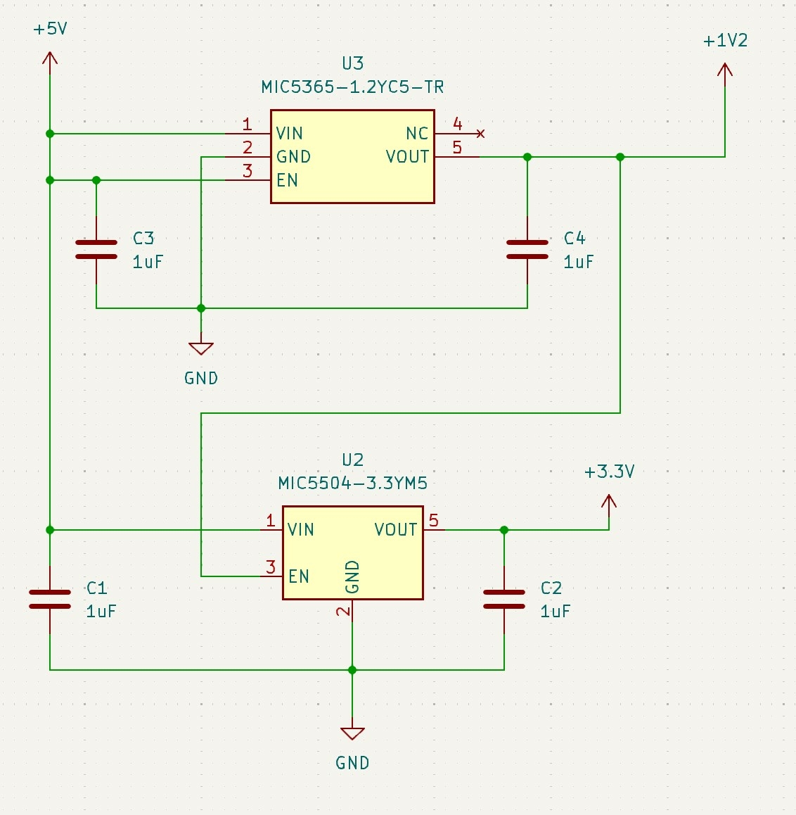
The first thing is to get the 3.3v, obviously. I will use a MIC5504-3.3YM5 LDO. The FPGA also need 1.2v for its core power. I'll use the MIC5365-1.2YC5-TR for that.
There is a note in the datasheet that says: "It is recommended to bring up the power supplies in the following order." Why is it just 'recommended'? Do they mean its not required but just good practice? Anyways, they say to apply VCC and VCCPLL first (1.2v), then the SPI_VCCIO1 (3.3v), the VPP_2V5 (3.3v), and finally the other supplies (3.3v). The TinyFPGA-BX schematics seems to do the opposite (https://github.com/tinyfpga/TinyFPGA-BX/blob/master/board/TinyFPGA-BX-Schematic.pdf), and the Lattice breakout board seem not to care (https://www.latticesemi.com/view_document?document_id=50700, p22 and 24).
To do what's recommended, this is what I think I should do:
(Connect the 1.2v to the enable pin of the 3.3v LDO to make sure we supply VCC before SPI_VCCIO1 and the others)But 1.2v is the minimum logic high voltage for the enable pin of the 3.3v LDO, so I'm not 100% sure if it's the way to go. Maybe I'll put some 0 ohms resistors to be able to switch to a configuration like the TinyFPGA.
Configuration Memory
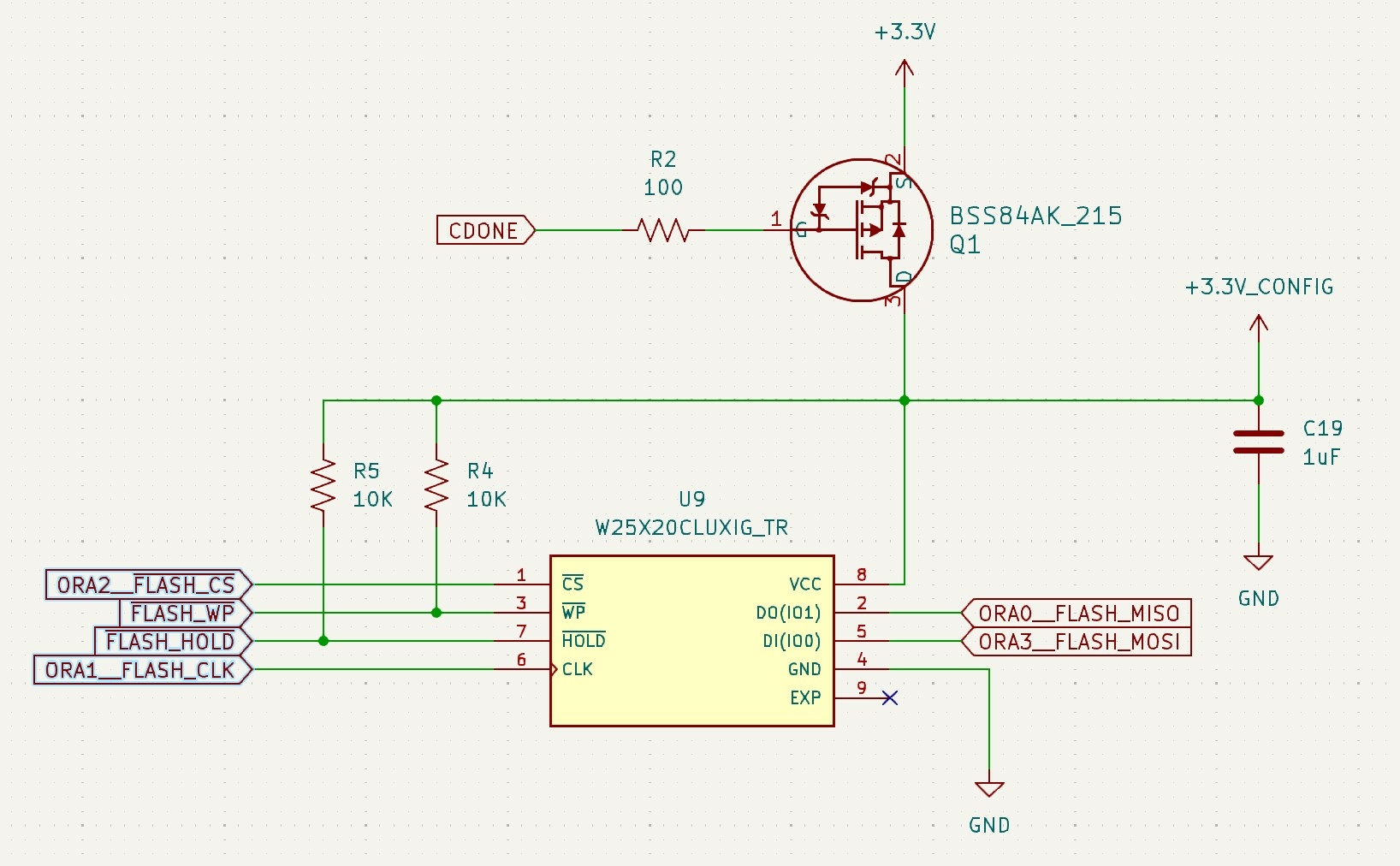
The iCE40 family FPGAs need an external memory to configure itself. I use a Windbond W25X20, and the FPGA can get its configuration directly from this Flash via SPI. (More on that later)
Pins and Level-Shift
The IOU has 19 outputs and they're the easiest to deal with; the 5v TTL will see 3.3v as a logic HIGH, so nothing needs to be done.
The IOU has 10 input pins. These must be shifted from 5v to 3.3v. I do that with a 74LVC541 (8 channels) and a SN74LVC2G125 (2 channels)
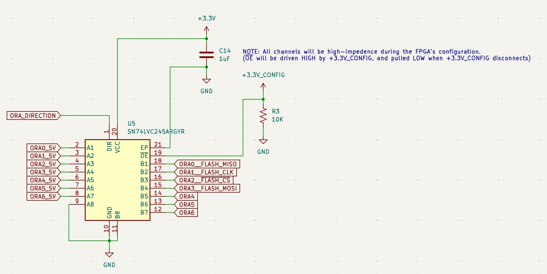
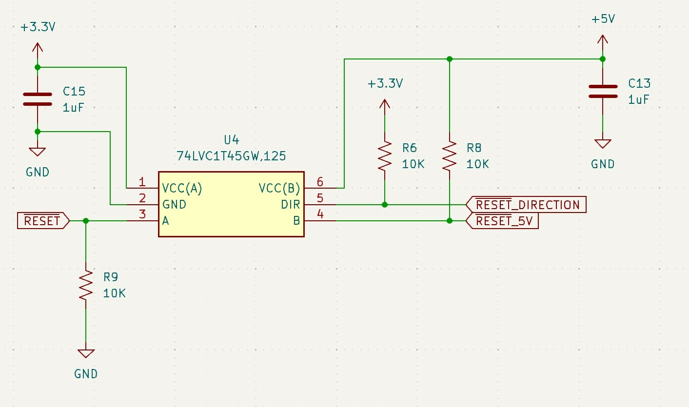
And finally, the IOU has 8 bidirectional pins; the /RESET and ORA(6-0) signals. They can be inputs so they must be level-shifted. I use a SN74LVC245 for the ORA, and a 74LVC1T45GW,125 for the /RESET. And since they are bidirectional, the bus transceiver need to know their direction, so we need 2 addidional pins: one for the /RESET direction, and another for the ORA direction.
More complications
So, we need a total of 39 pins; the exact number of GPIOs on the ICE5LP1K-SG48. That means we need to use the annoying dual-purpose SPI/GPIO pins. The FPGA use these pins to get configuration data from the Flash Memory during configuration, then drive the CDONE pin HIGH, and these dual-purpose pins become GPIOs. So, if we're not careful, the normal operations for the IOU can inadvertly issue read commands to the Flash Memory and disrupt the IOU signals. Alternatively, configuration data may leak outside the IOU replacement if we're not careful.
My idea on how to fix this is to use a pMOS to power down the Flash Memory once the FPGA configuration is done (CDONE High).
That way, the first of the two problem is fixed:
The other problem is preventing the configuration data from leaking to the outside. To fix this, I will use the SPI/GPIO pins to carry some of the ORA signals, and connect the power cut by the pMOS with the output enable of the ORA's bus transceiver.
Like this:
Even more complications
The last problem I see is with the /RESET signal. With an original IOU, /RESET will be an output pin, actively being driven LOW until its power-on is completed, then it becomes an input pin with a pull-up.Unfortunately, all GPIOs on the FPGA are Hi-Z during configuration. So we must pull /RESET LOW during the FPGA configuration, and then HIGH after (!). Plus, the direction will also be Hi-Z during configuration so it must be pulled HIGH (if we place the FPGA is on the 'A' side, and the Apple IIe is on the 'B' side). This is what I think will work:
It's not ideal because /RESET will be constantly leak current by being pulled down. But, given the space I have on the PCB, I haven't thought of anything better.
As you can imagine, we're far from a 5v CPLD adapter, where only the CPLD and a few decoupling caps are needed...
All comments are welcome!


- Power sequencing
This is the bane of all multi supply voltage ICs. It is mandatory, you must follow the recommendations in the datasheet, or your IC will blow up / get damaged at some point. It can be tricky to do this without a power supply management IC which supervises and sequences these power supplies. You can develop your own solution based on discrete components but you must do all the lab work to assure that under no circumstances of power up / power down ramps the IC ever "sees" the particular combinations of supply voltages on it which are the damaging case.
- Level shifting
3,3V CMOS ICs having PMOS high side drivers make enough logic swing for TTL. Check that you CMOS IC does not have NMOS high side drivers. These can't reach VCC when driving high. But some companies use that trick to prevent latch up or make a 3.3V part 5V tolerant on its outputs ... but 5V tolerance on an output does not imply it can be driven to VCC of the IC. Sneaky marketing bastards.
- Latch up
If you ever exceed VCC (here: 3.3V) on any pin (input or output) of your 3.3V IC - unless explicitely being advertised as 5V tolerant - than your IC will die from latch up, sooner or later (my money is on "sooner").
Too avoid, you may use series resistors which limit the current into the I/O pins which may see higher voltages than the VCC of the IC. Latch up tolerance is sometimes specified as how much current can be forced into a pin before the device goes into latch up (triggering a parasitic SCR within) and then blows up. Proper sizing of these resistors can be tricky when you need to drive TTL which draw some input current, or if you need to drive higher capacitive loads, where the RC time constant matters. But in general, having properly sized series resistors greatly reduces latch up risks. Some ICs need 50mA or more forced current to latch up, and it is easy to limit input/output currents to a safe level below that point, by means of series resistors. Unless you need to drive large capacitive loads fast, or too many TTLs. But the MMU only has 16 outputs. You can always add TTL or HCT drivers. HCT can latch up (like all CMOS) but no TTL (LS, S, AS, ALS) suffers from that, ever.
On inputs you can use resistive dividers in lieu of active level translator ICs.
You can make a beefy 3V shunt regulator and then use small signal Schottky diodes (PN diodes are too slow) as voltage clamps on inputs, and on outputs, after the series resistors (otherwise the Schottky diodes will blow up). The anodes of the diodes would be at the input/output pin, the cathodes at the shunt regulator for 3V. Depending on the type of the Schottky diode, they will turn on and limit further voltage rise before internal parasitic diodes within the IC can turn on - these parasitic diodes are PN junction diodes and they ALWAYS have a higher forward voltage than Schottky diodes. Theoretically, you could use the Schottkies as clamps against the VCC pin of the IC to be protected and still be safe. No shunt regulator needed. But then you should go for Schottkies with a small forward voltage of no more than 0.4V --- with a shunt regulator you are more flexible here. You can experiment with LEDs in lieu of the "shunt regulator" ... depending on the color they may have the right forward voltage already, and you can always add a PN junction diode to increase the forward voltage. Add a small "keep alive" current via a resistor to VCC, just enough to keep the current flowing but the LED still very lowly lit. When you work on such a PCB and the LED ever lights up, you can take this as a warning that something just has tried to kill your 3.3V IC. But it will be protected. The LED will swallow the excess. But the current limiting resistor must be there, else the LED may die in the attempt. I used that LED based clamp trick a lot when developing mixed voltage systems. It helps to identify offenders.
- RAS delay
In my MMU substitute I did that with an external RC. This is not critical timing. You could ask users of your MMU drop in to make a small wire from your MMU to the unused output of the TMG PAL. Which is "AX" and just the right signal to flick the address muxes between RAS fall and CAS fall. The wire is ugly, yes, but we want to be cheap. Your oscillator (unless it's a PLL) may introduce synchronization slips. No good. PLL will wreak the same havoc until they are in lock.
Bottom line
Why not use 5V CPLDs. Lattice ispLSI1016 still can be had from non-Chinese sellers, but of course, they are out of production. Before my Tower PC went down I had a MMU implementation in an ispLSI1016, with just one external 74xx257 MUX needed. But I never got to the end result, the PC died on me during this work. Need to repair this machine first.
- Uncle Bernie
Thanks UncleBernie, that's a lot of good info. I seem to keep switching back an forth between 3.3v and 5v as the better option, but the simplicity of the 5v option is pretty compelling -- only one component (plus decouping caps). I can't just give up on the 3.3v option, but given the complexity and the higher probability of making desing errors, this option is becoming less and less realistic.
I will try with the ATF1504AS and ATF1508AS.
Changing subject, for anyone who lands here searching about the iCE40 power-on sequence, while reading Lattice's own breakout board schematics, I found in a note of the iCE40 Ultra Breakout Board (https://www.latticesemi.com/view_document?document_id=50700, p.10):
So apparently, a proper power-on sequencing is only required if you intent to boot from NVCM. Why they didn't explain this in the datasheet baffles me.