I am starting this thread so I can ask for some feedback on my designs for an adapter for the IOU and MMU. As I mentionned in this thread: https://www.applefritter.com/comment/110444#comment-110444, ReActiveMicro originally offered to design the hardware for the replacement adapters. However, Henry told me recently that he wouldn't be able to work on this any time soon given his lack of free time. So, I decided to revisit an attempt I did some time ago.
The VHDL code for my project (https://github.com/frozen-signal/Apple_IIe_MMU_IOU) was developped using an ALTERA EPM7128STC. But, this CPLD is not produced anymore and the only way to buy them is to find them on places like eBay and AliExpress. The CPLDs that comes from these places are unlikely to be new ones; they are probably pulls or recycled ones in some way. So, each chip must be tested indivually to make sure it works. A tedious task. Besides, the irony of using obsolete CPLDs to replace obsolete ASICs don't escape me.
So, designing the replacement adapters with modern and active compnents makes sense. This is what is needed:
- A FPGA with at least 38 GPIOs and small enough to fit on PCB the size of a 40-pin DIP.
- Ideally, the FPGA should have an internal oscillator to generate some hold delays that the Apple IIe requires.
- All the components must be active, inexpensive and easy to source.
- The PCB must only require basic PCB manufacturing and be relatively easy to assemble for a hobbyist.
The Lattice iCE40 FPGA (ICE5LP1K-SG48ITR) fits that bill; a 7x7 mm, QFN-48 package that is very popular with the hobbyists and has an internal 48 MHz oscillator.
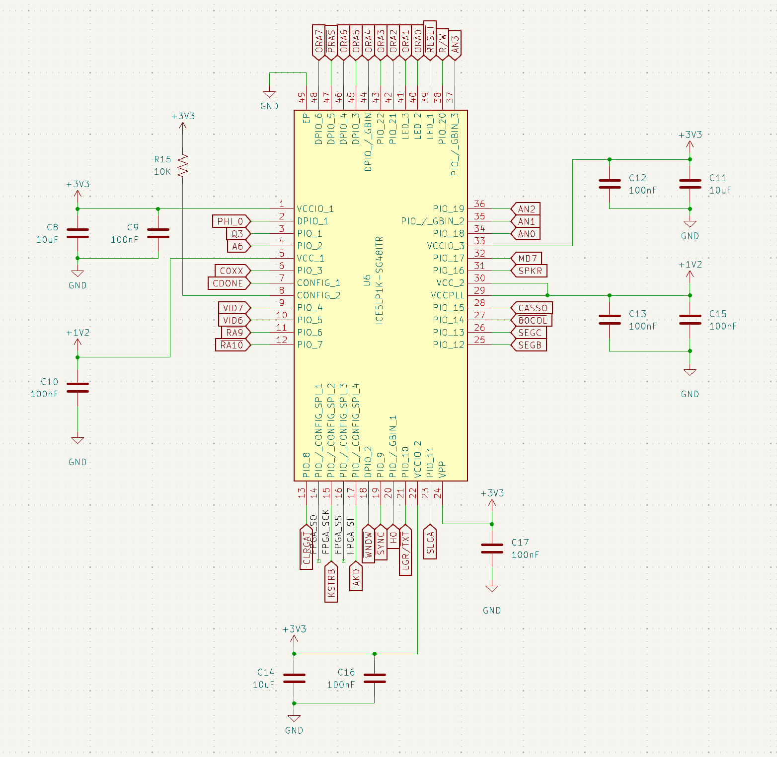
On the downside it's a 1.2V device with 3.3V banks, so every inputs and bidirectional signals need to be voltage level shifted down to 3.3V. The main challenge is to fit all the level translation onto a PCB the size the official IOU and MMU.
Also, although it has enough GPIOs, 4 of them are shared with the configuration pins. For those unfamiliar, this means that when the iCE40 is powered on, it uses 4 special pins SPI to read its configuration data from a Flash Memory IC. Once the configuration is done, these 4 pins becomes available as GPIO.
Note the KSTRB and AKD signals that are shared with FPGA_SCK and FPGA_SI respectively, more on this later.
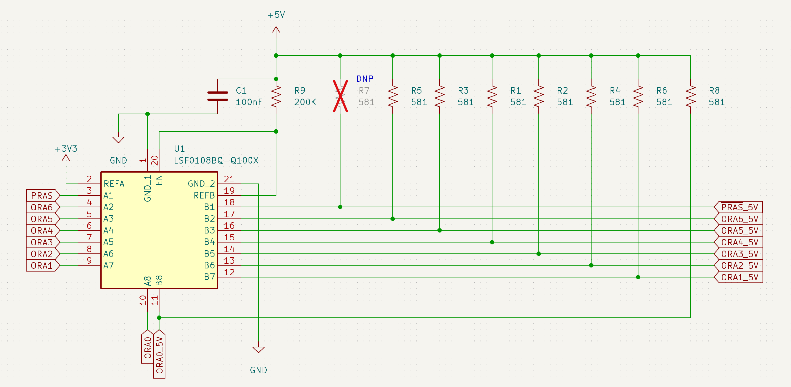
For the bidirectional signals ORA6-0, a LSF0108 is used for level-translation. This device don't need a direction pin which is really good, but need a bias resistor (R9) and a pull-up for each channel on the high-voltage side (see table 9-3 of https://www.ti.com/lit/ds/symlink/lsf0108.pdf to understand where the value of 581 Ohms comes from). /PRAS is an input-only signal but is routed through this component because a channel was free. This is why R7 is DNP; the pull-up is optional for an input signal, but the footprint will be there if needed.
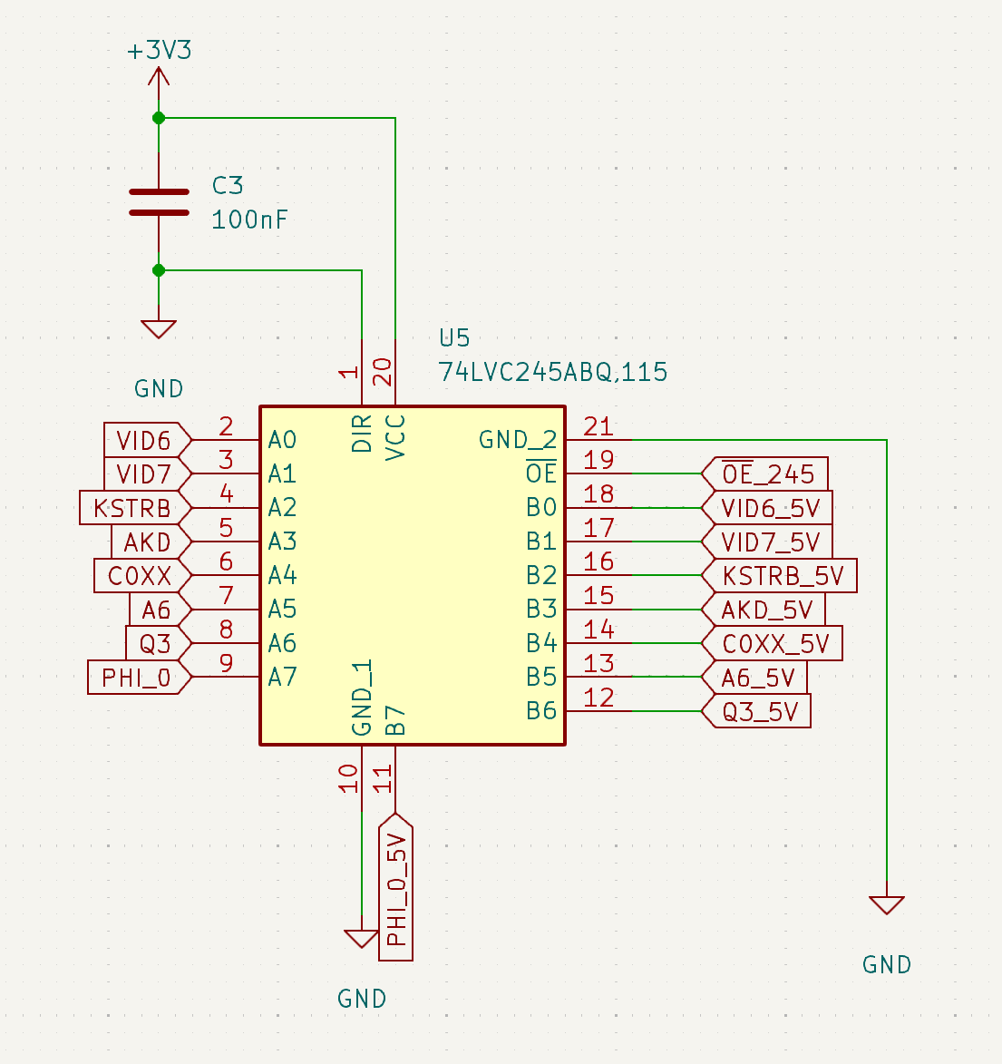
The LVC245 level-shift input-only signals and would be pretty straightforward if it was not for KSTRB and AKD. These two signals are shared with the FPGA SPI pins and we must make sure that external KSTRB or AKD signals don't mess with the SPI signals during the FPGA's configuration. The way to do it is to disable the LVC245 with /OE during configuration time.
I use CDONE, this signal is LOW during configuration and driven HIGH in user mode. Unfortunately, that's the inverse of what we need, we'll have to invert CDONE:
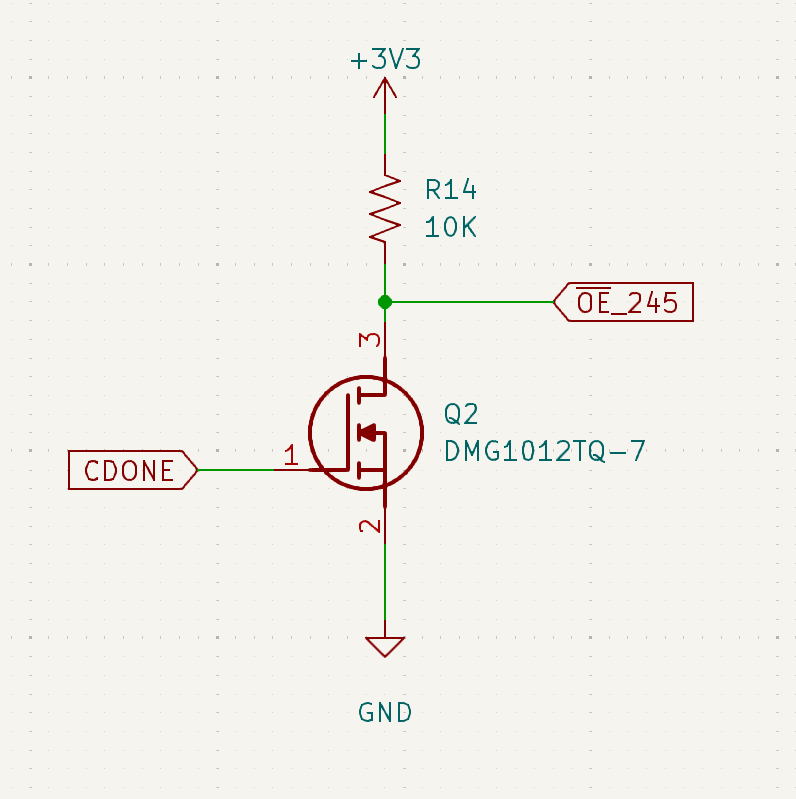
Here, when CDONE is LOW, the NMOS will be in a non-conducting state, and /OE_245 will be pulled-up by R14. When the configuration has finished CDONE will be driven HIGH and the NMOS will turn on driving /OE_245 LOW.
I could also do it with a GPIO:
- Move an input pin to FPGA_SO (FPGA_SS can't be used because the Flash Mem need to remain unselected in user mode)
- Pull-up that freed GPIO. During configuration, all GPIOs are placed in a high-impedance state.
- Configure that GPIO as open-drain and drive it a constant LOW in user mode.
I just preferred to use the FPGA's CDONE signal with an NMOS.
I use the DMG1012TQ-7 because it's small, it's logic-level (VGS(th) = ~0.75V) and has low RDS(on). Plus, it's inexpensive and places like Mouser have these in large quantities.
The /RESET signal also need special handling:
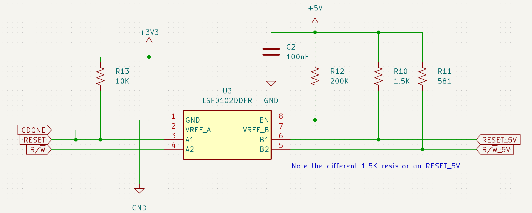
In the official IOU, this signal is an open-drain pin with an internal pull-up. To level-shift these with a LSF010x, a pull-up is required on both sides. And since GPIOs are in a high-impedance state during configuration, that means /RESET will be pulled HIGH during this time, and this is not what we want. The fix is simple, fortunately: CDONE is itself an open-drain with weak pull-up, and shorting CDONE with /RESET will give us the desired behaviour.
The remainder of the schematic is standard stuff:
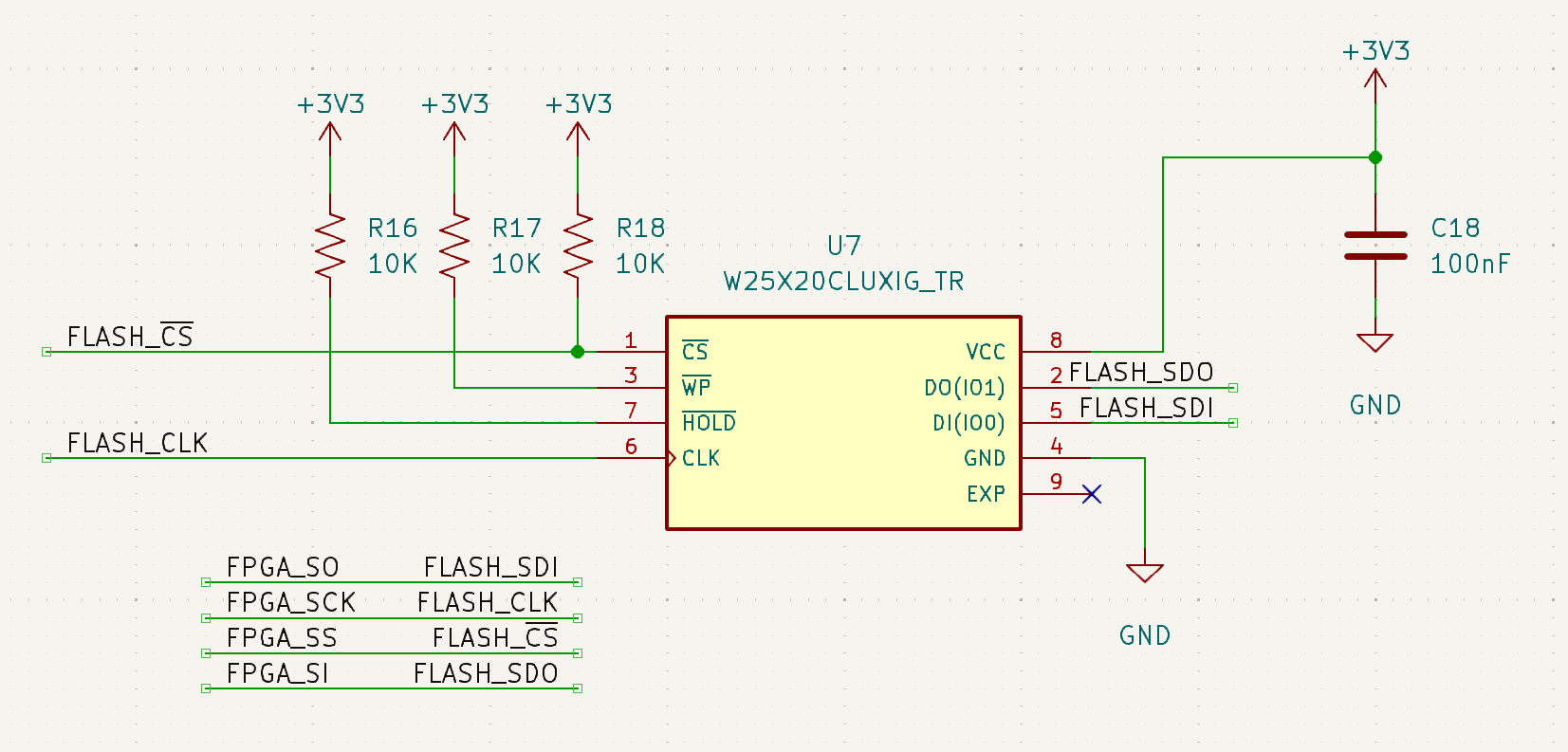
- A Winbond W25X20CLUXIG Flash Memory: a SPI Flash module that is small, inexpensive and in ample supply. Note that CLK and DO are tied to KSTRB and AKD respectively. During configuration, KSTRB and AKD won't mess with the SPI signals because as seen earlier, the LVC245 will stop outside's KSTRB and AKD from messing the data. And once the configuration is done, /CS will be held HIGH and CLK and DO signals from outside will be ignored.
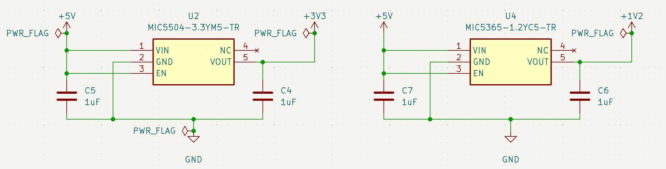
- MIC5504-3.3YM5 and MIC5365-1.2YC5 LDOs are used to convert 5V to 3.3V and 1.2V. I used these because, like the other components, they are small, inexpensive, easy to solder and easy to source.
There are two problems with the current design: CASSO and SPKR are tied directly to the adapter's pin and are 3.3V. Since these two aren't used as logic signals, I may have to level-shift them to 5V. SPKR is amplified and may be okay, but CASSO probably won't be.
Assembling:
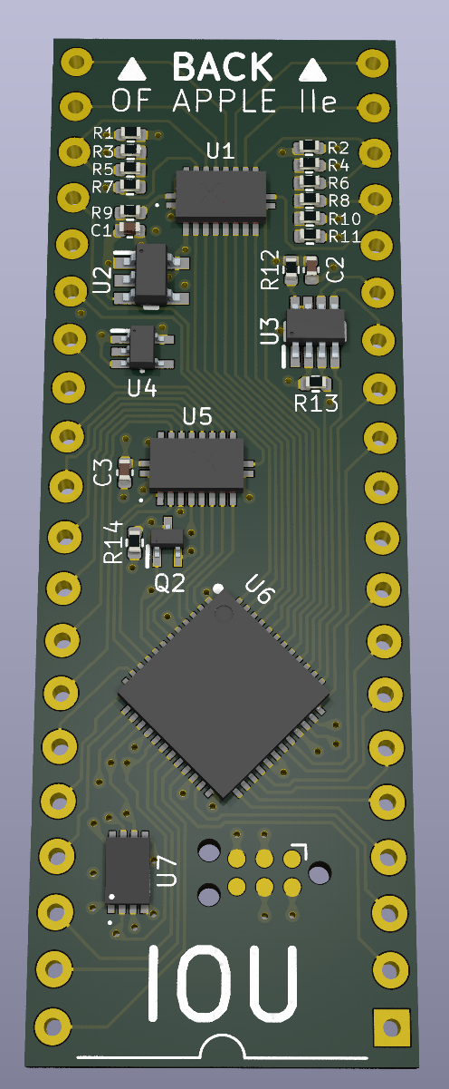
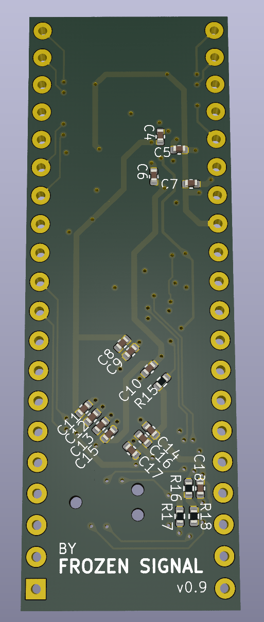
I moved components to the front side as much as I could, and only resistors and capacitors remains on the back. So, the easiest way to assemble the adapter would be reflow the back first. Then, only light 0402 components will be on the underside during the second reflow cycle, minimizing solder joint sagging. With a hot plate & hot air, I think the best way will be to reflow the front, and then solder the back with hot air.
Finally, just like the VHDL part of this project, I plan to upload the Kicad schematics on github once I know they works. I will use the same license (Creative Commons Zero) so that anyone can use them in any way they want. And as a sort-of disclaimer, I have no intention of making money from this project, and I have no problem if other people makes money from this project.
As always, any thoughts are very welcome.
Hi,
SPKR sould not be a problem as the amplifier is class C. For the CASSO there is a voltage divider and the output is app. 41mV; with 3.3 it will be 27mV... Might still work as the s/n ratio would be quite good.
Lesson learned ;) https://www.applefritter.com/comment/110457#comment-110457
Oh yes, I see this now about the switching mode, nice! :)
Hello Frozen signal,Thank you for your IOU/MMU project.
I'm trying to create my own replica of Apple IIE (mentionned in this thread: https://www.applefritter.com/comment/110461#comment-110461 ) using your VHDL code. I am using Quartus II 13.0.1 and EPM7128SLC84-15 as CPLD for MMU and IOU. I wanted to ask if it's normal that I get multiple warnings about inferring latch(es) during compilation like this:
Also of concern are warnings such as:
I would like to understand, is this how it should be, or am I doing something completely wrong? I have already received the PCB and partially assembled it, but something is not going as I would like, especially in terms of image output and working with DRAM memory...
"Inferring a latch" is what the silicon compiler is forced to do when the HDL code assigns a value to a signal in some branches of a process but not in others. If the signal's value is determined only by the inputs at the current clock cycle, it can be generated entirely by gates (implemented by LUTs in the FPGA). If its value might be "held over" from the previous clock cycle without change, it's necessary for there to be someplace to store the old value, which must be a latch.
Where the designer knows that a value must be stored across cycles, the proper way is to create a register in the HDL. No warning about inferring latches will be emitted in that case.
A "combinational loop" is another type of problem where there is a mutual interaction between signals. If you define A = B, and B = not A outside of a clocked process, you have created a free-running oscillator. This can make the circuit behavior nondeterministic.
Both types of warnings are indications that there is a bug in the HDL code. Signals should only be updated in clocked processes and defined within every branch of the process.
I partially disagree with robespierre; these warnings is just the compiler telling you to check if that's what you want, and not necessarily latent bugs. "Inferring a latch" is indeed a signal that is mapped to a latch, but in the case of the MMU and IOU, that's what we want. I agree though that ideally all processes should be clocked, but most of the MMU and IOU is async and we have to do the same.
For your problem with DRAM and image output, if you have an oscilloscope or a logic analyzer, the fix will be easy. The hold times must be adjusted.
To fix, hook your scope on PHI_0, /RAS, Q3 and RA0. Check the time between the falling edge of /RAS (during PHI_0 in the case of the MMU and PHI_1 in the case of the IOU) and when RA0 change value (t_RAH). Do the same thing for Q3 (t_CAH). In your DRAM_HOLD_TIME.vhdl (assuming you're using the one with LCELLs), adjust NUM_LCELLS_RAS and NUM_LCELLS_Q3 so that t_RAH is between 32ns and 80ns, and t_CAH is at least 20ns (with a max of ~275ns). This file is used in both the MMU and the IOU, so fix the MMU and the IOU should be fixed at the same time.
See: https://github.com/frozen-signal/Apple_IIe_MMU_IOU/tree/master/CUSTOM/DRAM_HOLD_TIME
The hold delays in MMU_HOLD_TIME.vhdl are for /EN80, /ROMEN1, and /ROMEN2. The hold delay for /ROMEN1 and /ROMEN2 is not necessary; it's just added to be similar to the real MMU. So, do the same thing as before, but for /EN80 making sure the delay between PHI_0 changes and /EN80 changes is about 45ns.
See https://github.com/frozen-signal/Apple_IIe_MMU_IOU/tree/master/CUSTOM/MMU_HOLD_TIME
What exactly are your image output and DRAM problems?
And congrats on your project!
Thanks for answer, i have carefully studied the documentation on the MMU/IOU project website and read about NUM_LCELLS_RAS and NUM_LCELLS_Q3. Yes, i am using Altera's LCELLs, so first of all I try to use your default values (LCELLS_RAS=14, LCELLS_Q3=10). I connected the logic analyzer to the main signals and saw the following picture:
ras.PNG
So, t_RAH with default settings is 18ns
q3.PNG
and t_CAH is 33ns. I tried increasing the values NUM_LCELLS but haven't achieved any success yet. I'm also confused by the appearance of some glitches on RA0....
I don't know -) I am starting with appleII deadtest ROM ( https://github.com/misterblack1/appleII_deadtest ) in this case the behavior is approximately as follows: short video . I also tried to run the PCB with a A2VGA video card, and it sometimes showed some signs of life:
photo_2025-01-15_19-32-24.jpg
photo_2025-01-15_19-44-20.jpg
photo_2025-01-15_19-44-57.jpg
I am concerned about glitches on RA0 - I can't figure out what is causing them yet. Maybe a bus conflicts on the ORA between MMU and IOU.
May be I'm wrong, but it seems your 14Mhz clock is actually 66Mhz regarding timings that you show.
Good catch rumburak!
Tronix, this looks more like signal noise than contention.
If I were you, I'd make sure the MMU and the IOU works on an actual Apple IIe first.
Make an adapter and hook your MMU on the Apple IIe and make sure it work. Then do the same with only the IOU. Then both together, and finally with a 80-col card. Only then I'd try to make them work in your motherboard.
Here is my hw, based on EPM7160STC100:
20250117_103349.jpg
20250117_105008.jpg
I have problem with some CPU from different manufacturers.
When use both emulated MMU and IOU and test with internal ROM test (Apple IIe ROM and enhanced IIe ROM) it fail for MMU.
Test pass with: SY6502, R65C02P2, some newer CM630 (Bulgarian clone).
Fail with: UM6502, G65SC02P-2, some older CM630.
Thanks rumburak! I'll try to find some of those CPUs that fail and update my repo.
Thanks guys, i really did not grab the signals correctly - it's all because of the not very useful chinese software for my cheaper logic analyzer. So, 14 MHz is 14,3xxx MHz, previous pictures (with timings) are not correct, sorry about it.
The problem here is that i don't have Apple IIe, that's why i want to make it -)
At the moment i managed to achieve that I pass first time the deadtest without memory errors with an external A2VGA video card:
photo_2025-01-18_19-53-38.jpg
The next cycles produces errors in the 5x and 6x range:
photo_2025-01-19_18-58-44.jpg
When i started board with Apple IIe ROM its passed external mem test and finaly says "IOU" at the center of black screen.
But when outputting an image from the board, I still get a flickering noise similar to the one in the previous video. Therefore, my assumption is that the MMU seems to be working, but there are some problems with the IOU.
rumburak ,i would like to ask how you used the Global Clock (PIN_87), Dedicated input (PIN_90) pins in case of EPM7160, or you didn't use these "special" pins? In my design i connect PRAS to usual I/O, then PHI_0 to Global Clock and Q3 to Dedicated Input on both MMU and IOU - maybe this is a bad idea. Maybe I should connect all these signals to regular I/O pins and don't use "special" global signals?
Do you know Andrei, the director of the Apple Museum in Moscow. If necessary, I could ask him to help you with testing on a real machine. I would help you myself without any problems, I have an Apple //e but I live in Samara.
Pins like the Global Clock are special pins that are routed inside the CPLD in a way to minimize skew between logic elements. Normally a good thing for clock signals, but in the case of the MMU and IOU, the frequency is too low to make any difference. Pick whichever pins are the most convenient to you.
How did you source your CPLDs? I remember early last year having bought on AliExpress several bad EPM7128STC. Some couldn't be programmed, others had very bad noise on some pins maybe a bit worse that what I see on your captures. (Change the code to output a constant LOW on one of the pin, and a constant HIGH on another. Are they noisy too?) I had one of these CPLD fail in a way that looks a bit like your video. All this to say that there is a possibility that you have bad CPLDs.
Also make sure your DRAMs are working. Swap them around and see if the problem 'follows' one (or more) of the IC. A bad DRAM chip is a common failure in the Apple IIe. There is even a brand of DRAM that is notoriously unreliable. They were manufactured by Micron Technology and if you have any of those, don't waste your time; they all go bad. Just remove and replace them. Do a Google image search for "Micron Technology MT 4264" to see what they look like.
One last thing: How other outputs from your IOU and MMU looks like? Do they all have that signal noise? And what do the inputs look like? And look at some signals that don't go to / comes from the IOU or MMU.
Again, good work Tronix! I'm sure everything will work fine once you fix the signal noise problem.
I got the CPLD chips partly from Aliexpress (suspicious markings) partly from the local market old stocks (original Altera's 100%). I tried both and they all behave the same. They programming normaly, there is no noise on the output pins with constant ('1' or '0') values. I have heard about the famous MT-ram chips, but i do not use it. I use old Soviet chips pin-to-pin compatible with 4164.
And yes, i finally got it!!!
photo_2025-01-21_16-20-48.jpg
I put 220pF capacitor between 1st pin 74LS374 (PHI0) and GND and it fixed all my problem. Board is passed deadtest with unlimited cycles count (currently running over 12 hours). Short video: https://disk.yandex.ru/i/6TOtQePHvauFUg
I also managed to run Apple IIe enhanced ROM promt. I can't check it further yet, because I need to write firmware for the keyboard controller.
Anyway, thank you all so much for your support. Thanks frozen signal for your great VHDL MMU/IOU project again.
On your Apple ][ motherboard you can prepeare a bootable diskette and start any file based game without keyboard. Many of these games have demo/introduction mode that runs until keypress, e.g. without keyboard. Later make sure your capacitor clock tap does not lead to incompatibility with ramworks or other peripheral cards. I am still highly suspicious about compatibility of these PLD replacements after my own experiments with them. Let's hope things are improving gradually. Had you had copied the keyboard interface from Pravetz 8C schematics, there was a ready-made interface based on Microchip PIC to PS/2 keyboards made by Rumburak many years ago. I hope he can share his code and project, but better ask him. I have also dumped successfully the CM650 (masked variant of MC68705P3) code from Pravetz 8C/8A keyboard (within the keyboard assembly) controller, and of the GI's KB9600-PRO and ported later to modern DIP40 PICs but pinout is different from the AY-3600 controller, anyway both serve a matrix keyboard direct connection. Writing from scratch new firmware for a keyboard controllers should not be a difficult task.
Hello FrozenSignal,
A long time ago I promised you some tests for the graphics side of the IOU. After a lot of work, I'm now emulating that in great details and can share my test cases. Rendering of the test on my colour CRT:
IMG_3283_v1.JPG
and Accurapple emulation:
screenshot_crt.png
The corresponding code for these tests is there: https://gitlab.com/wiz21/accurapple/-/blob/main/composite/tests/logic_ana/lagr/la_gr.s?ref_type=heads
In post #17, 'Tronix' wrote:
" I also managed to run Apple IIe enhanced ROM promt. I can't check it further yet, because I need to write firmware for the keyboard controller. "
Uncle Bernie comments:
I'm also writing code for a keyboard controller right now, for my YAAK keyboard which has an on-board scanner, but no encoder yet. My idea is to design and develop a modular keyboard solution, which plugs into the Apple-1 or Apple II 16-pin keyboard port, but split the keyboard and the encoder. Other than the YAAK, the encoder should also accept a normal PS/2 keyboard which are cheap to buy and still being made (despite you would think that USB keyboards have taken over all of the market).
I intend to make the encoder as cheap as possible by using a small PIC 8-bit microcontroller. I'm just at work stripping down my "C" code for the PS/2 encoder by removing unnecessary key combinations. This normally is done in the BIOS of the PC and not by the PS/2 keyboard itself. So the original designers did not need to care to keep the code small, and there are many weird key combinations of ALT, ALT GR, SHIFT and CTRL which are useless for the Apple-1 and Apple II. On the PC, these generate key codes prefixed by a zero byte. For instance, the F1-F12 function keys have four different sets of codes depending on whether they are pressed alone, or with SHIFT, or with CTRL, or with ALT / ALT GR. These code sets are irregular enough to make the encoder software bloat up, and so I will surgically remove them from my code.
Once I have the PIC code, I will make it 'open source', so if you are short of time for your project, you can adopt it.
- Uncle Bernie
This does not relate to PC(AT/PS/2) keyboard at all! Such combinations are NOT trasferred over the keyboard cable to PC. There are only make/brake (press/release) codes per key irrelevant of other key states! You don't know what you are talking about, or you are stripping someone else's code.
I also thought about choosing a cheap microcontroller and chose AT89C52 (8051 core). It's retro, just like PIC8/16. It's cheap, they sell it by the dozen on Aliexpress for a very modest price. It has enough pins (DIP-40 package) to support a Apple IIe matrix keyboard without an encoder. It's five volt.
Yes, it is not very convenient for debugging, but I think I can manage somehow, sending debug info throught UART.
On my board I have provided space for installing a sandwich board with a keyboard controller, it is universal and can be services both PS/2 and original Apple IIe matrix keyboard. I am currently developing firmware.
photo_2025-01-23_08-50-50.jpg
In post #21, 'retro_devices' wrote:
" You don't know what you are talking about, or you are stripping someone else's code. "
Uncle Bernie responds:
Sentence deleted - Tom In my post #20 I explicitely wrote about the origin of these weird encodings:
" I'm just at work stripping down my "C" code for the PS/2 encoder by removing unnecessary key combinations. This normally is done in the BIOS of the PC and not by the PS/2 keyboard itself. "
So I am well aware that these weird encodings are generated by the BIOS, not by the keyboard itself. Oh, and I don't waste my time with "someone else's code" - I wrote the first version of my "C" encoder in the 1990s, but I'm trying to do it again with less substitution table space, to make it fit into a smaller microcontroller.
The purpose of my code back then - same purpose as now - is to have an encoder which takes the scan codes from an PS/2 keyboard and turns them into the same 'encodings' as the BIOS of the computer normally does: this includes all the SHIFT, CTRL, ALT, ALT GR, CAPS LOCK, NUM LOCK etc. modifiers and also the 'direct code' entry mode for arbitrary hex codes.
Even an idiot should be able to understand that the PS/2 keyboard without a substitute for the keyboard BIOS functionality is useless for Apple-1 and Apple II applications, as a PS/2 keyboard does not produce ASCII codes and strobe signals by itself.
Needlessly insulting paragraph that even misidentifies the person Bernie is trying to insult deleted - Tom
- Uncle Bernie
No need to throw shit on the fan, let's be a little kinder and more tolerant of each other.
PEACE - FRIENDSHIP - CHEWING GUM :) !
Long, ranty, insulting paragraph deleted - Tom
…(I was censored once here about this)… Twice - Tom
If there are insurmountable differences between you, I propose to solve them in the only way worthy of a nobleman, a duel. Choose pistol or sword.
Seriously, it's funny to read you, like grown-up people, but you behave like little children. A trowel in the sandbox did not share ... Solve your problems in private correspondence.
Being so peace challenging Russian you seem to be far away form your native country Russia that is at war now? It is funny to see what Western world embargo causes now again -- causing attempts to clone such obsolete but still otherwise widely available computers now by Russians, like in the late 80s and early 90s when all sort of Sinclairs, and similar by the time morally old computers were hand made/copied in Russia while the rest of the world's average user was enjoying the 32 bit 386/486 PCs...
Owad, you censored my message, my time to write here for an Nth time, I know you from the past 10 years now, that's your ugly way of closing free minds. But why have you left the same quote in my very message that leaves Grand bernie's words. Here is a copy again of my message then, I kept it, cause I knew you would delete it, and by the way I don't care if I have acount in such sensored forum, anyway:
Grand Grand Bernie, the one that has no knowledge of hiding his traces in internet, due to lack of knowledge on Ethernet/IP protocols, and attends daily a library to use public internet is you. Who is laways blaming his lack of time, failing PCs, software licensing, EU customs authorities, all but himself and his own society (I was censored once here about this), for not doing his job. Always stretching theories here, and everywhere, too much of bla-bla, more of writer than reader, and nothig productive. Nothing finished like it should be for finished devices. And on top of this inability to finish his devices, you are the only one thining they are something very precious, while actually you are inventing most of the time "hot water". Now you are covering with wordy text you understood your mistake, and blaming me an idiot are trying to force the Owad to remove all these messages, among which is not so hidden your technical incompitence. Without any proof, of course. Actually the one with aging brain pathology seems to be you (so far, unfortunately, I am close to this problem maybe too, time passes fast) Considering you attended socialist block countries in the past you seem to had been working for some covert services back then, sort of semi-engineer , semi - policeman. I know these people on the other side of the iron curtain, seems they were not different. They just had less resources.
While these sorts of personal vendettas are of course as interesting as a highway accident, there may be more productive ways to use our time.
I am opposed to censorship too, but it doesn't hurt us to consider the resources used by our communication and whether they are upholding their stated purpose.
I also don't believe, although the thought is attractive, that scientists/engineers from the west who traveled to socialist countries were all working on behalf of spy agencies. Many genuinely wanted to help create peace by establishing professional and academic relationships. It may be that they were ultimately undermined and misused by the state, but that doesn't impeach their motives.
It's the middle of the workday and I don't have time to comb through this discussion tracking down every petty insult. This thread is locked. retro_devices is banned for three months for repeated violations of the AUP.