
Hello everyone!
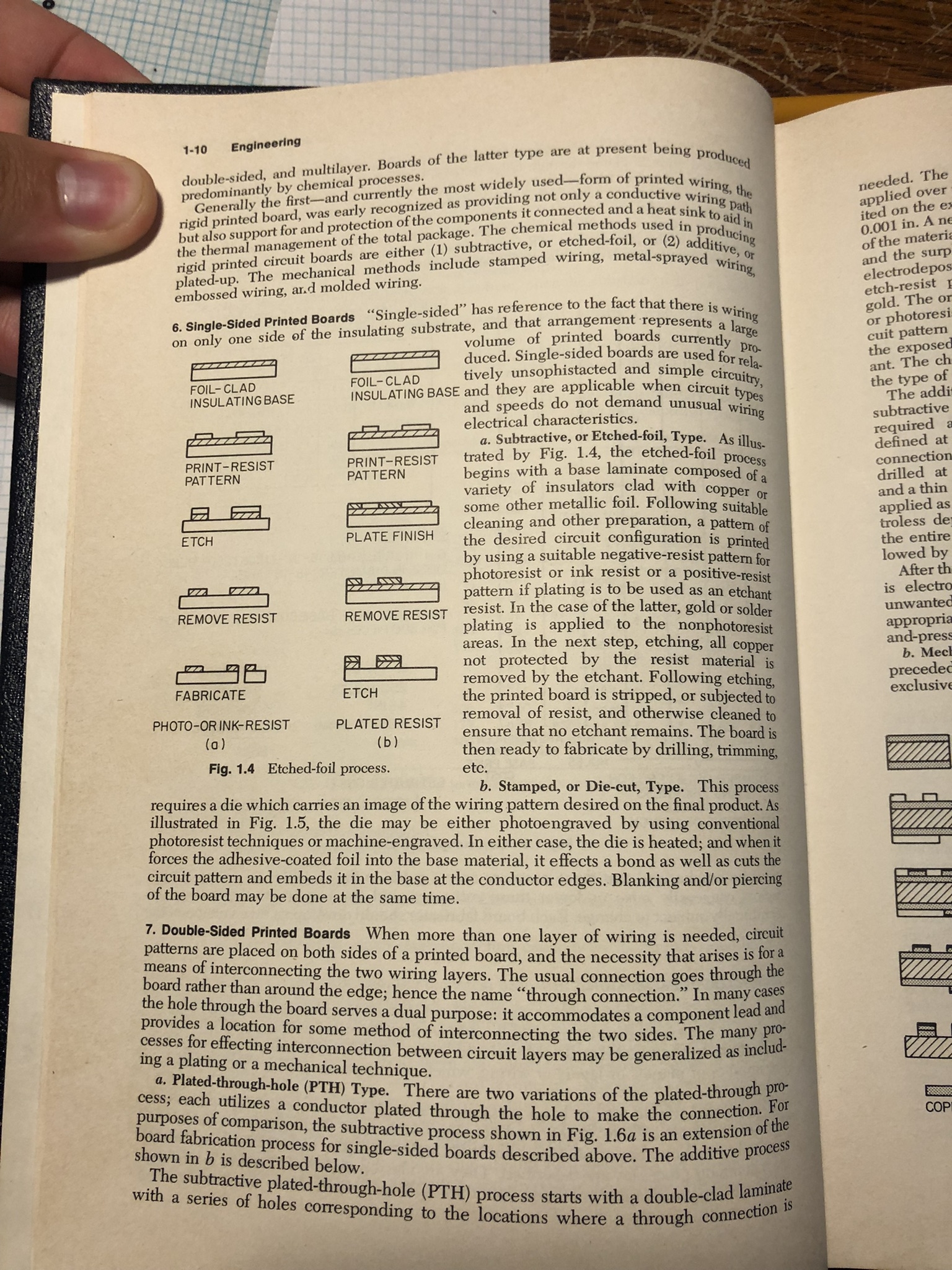
So, I have a project that I have been working on for months, and I have been researching just about everything there is to know about making literal PCBs (the old way), and also researching about how to draft board layouts for PCBs. So, I probably started this project in mid-august, and I bought a book called, "Coombs' Printed Circuits Handbook (Second Edition), and when I tell you this book has a WEALTH of information, it really does. This book has been CRUCIAL to learning about how these processes were done and how to do them. There are 7 sections with 4 chapters a section in this book, that teach about drafting the board, to making your PCB substrates & attaching copper foils to them, to making a screen printing setup, to screen printing on your own soldermasks & silkscreens, all the way through the processes of etching, and chemical baths, etc. AND IT'S ALL SO FASCINATING! Disclaimer, you will hear all of these months of work compressed into one post.
After reading extensively in this book, I have truly learned a lot, and also with the amazing help of Uncle Bernie as well, he had actually sent me some real drafted layouts that he had done back in the mid-80s and it really helped me get a sense of how much work went into drafting a board layout. So, the reason I say the post is about the Apple-1 is because, of course I would like to draft up the Apple-1s board layout, and I know that there will be people that will think to themselves, "why?", my answer consists of three reasons, #1. Because I can. #2. Because it will be a MASSIVE teaching of immense knowledge for me to learn at 18 years old. #3. It also would allow me to make the MOST highly accurate replica EVER! Which is an incredibly motivating personal goal of mine, also I'm aware of tha whole "possible forgeries being sold" debate, but honestly, those conversations are entirely subjective. If anybody truly thinks that after my boards are made and suddenly my boards come across someone who thinks they are real and tries to sell them, is is THEN the BUYERS own responsability to do the proper research to determine it's authenticity. If they call in an expert, for example Corey Cohen, there will be "markers" on the board that will indicate that it is a replica. So, let the record SHOW that there WILL be a way to tell that it is a replica, regardless of what anyone says.
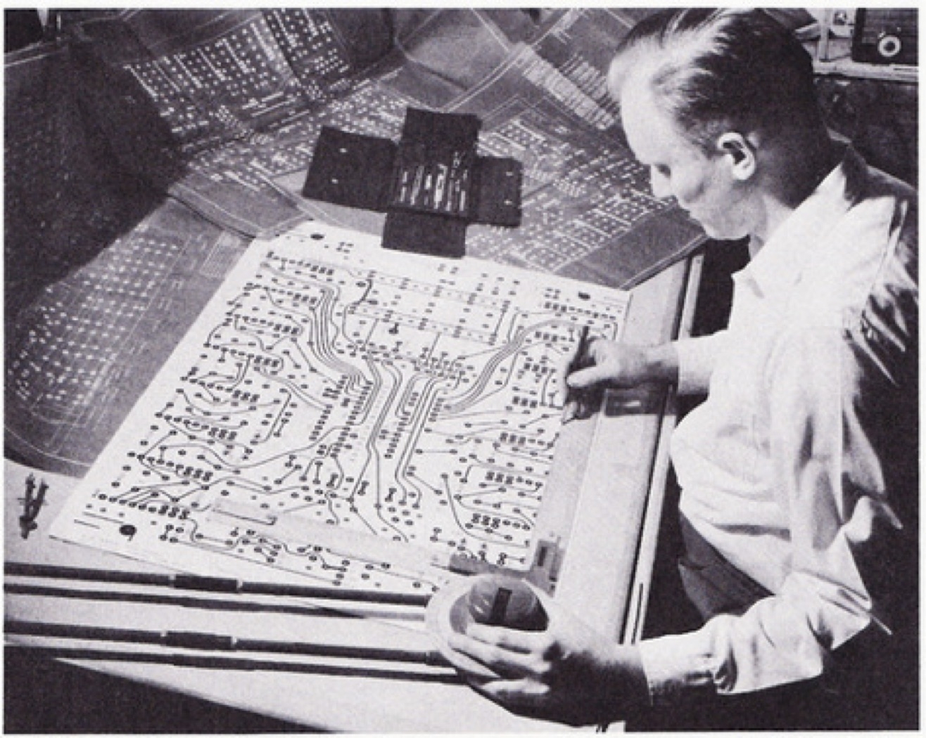
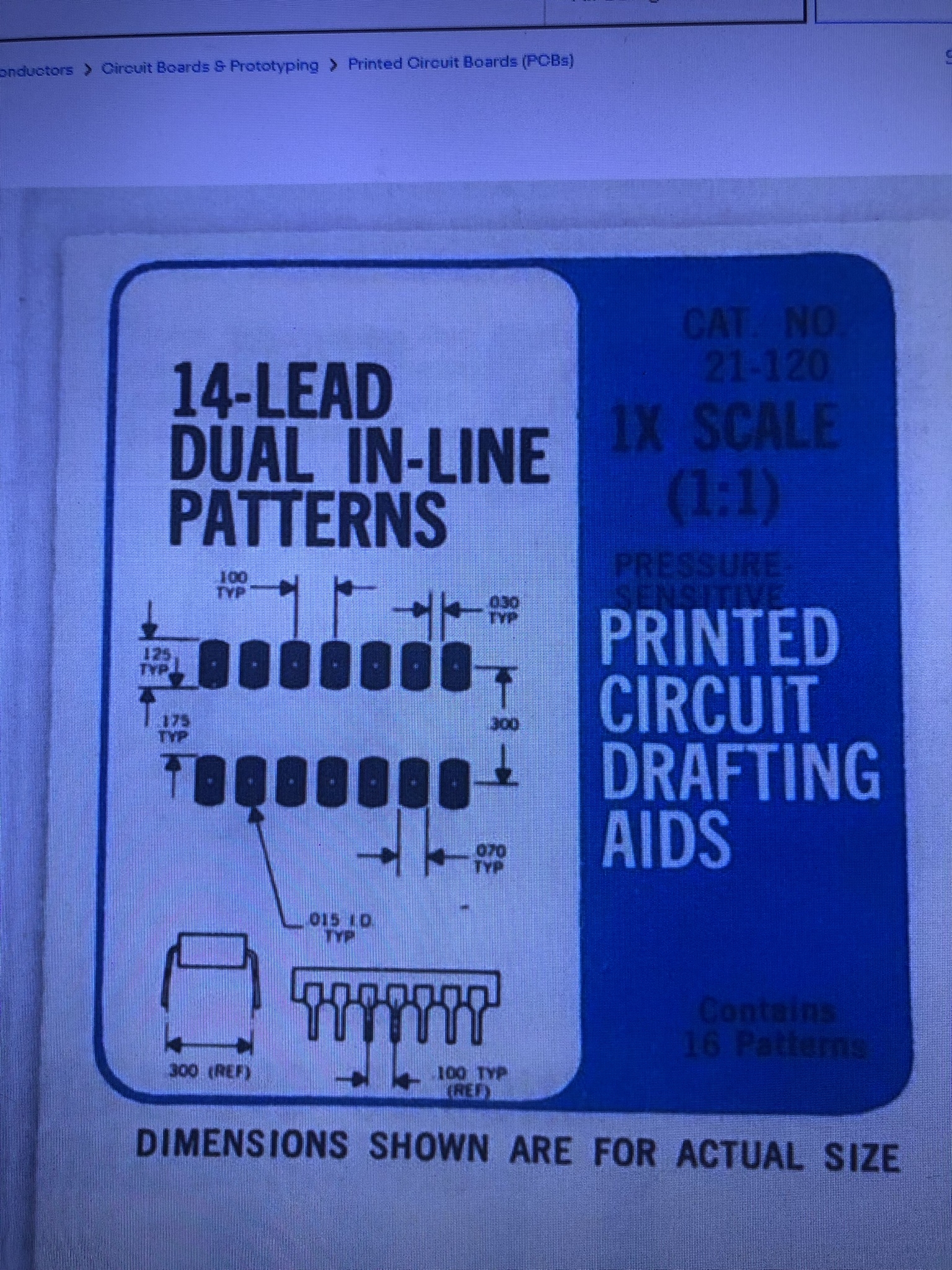
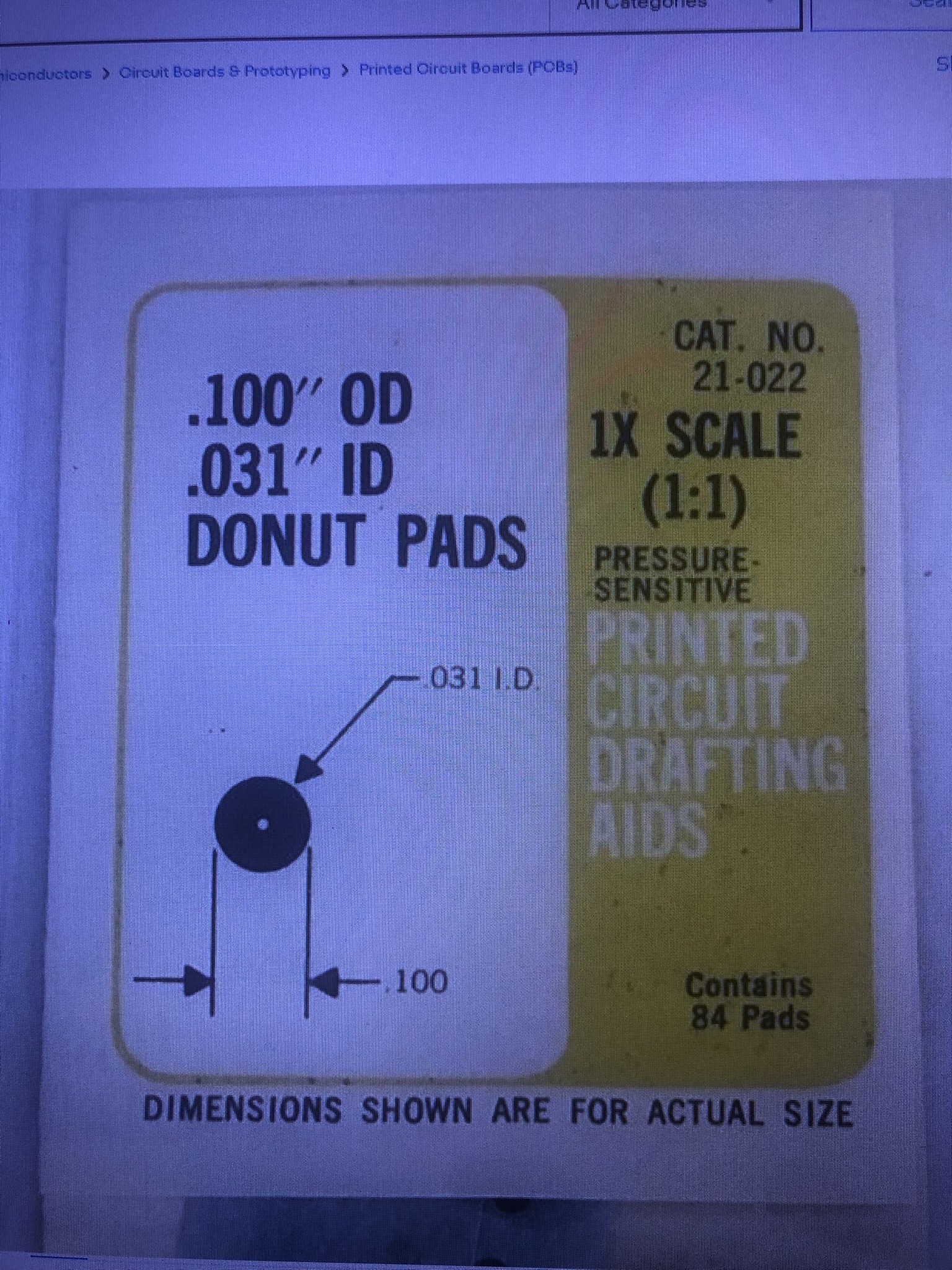
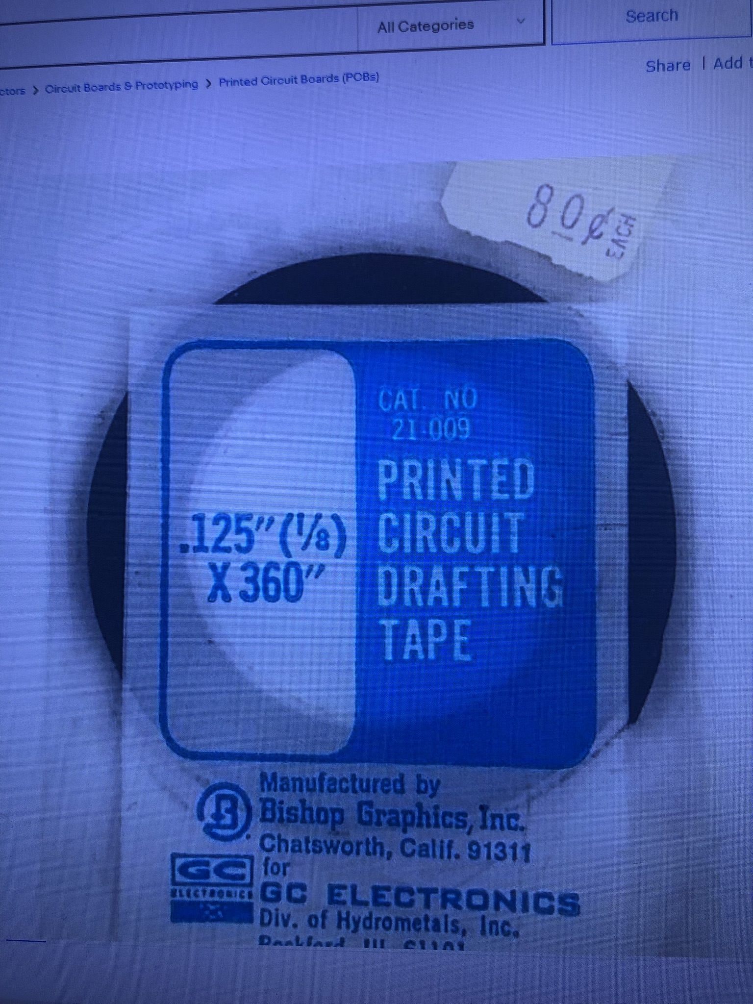
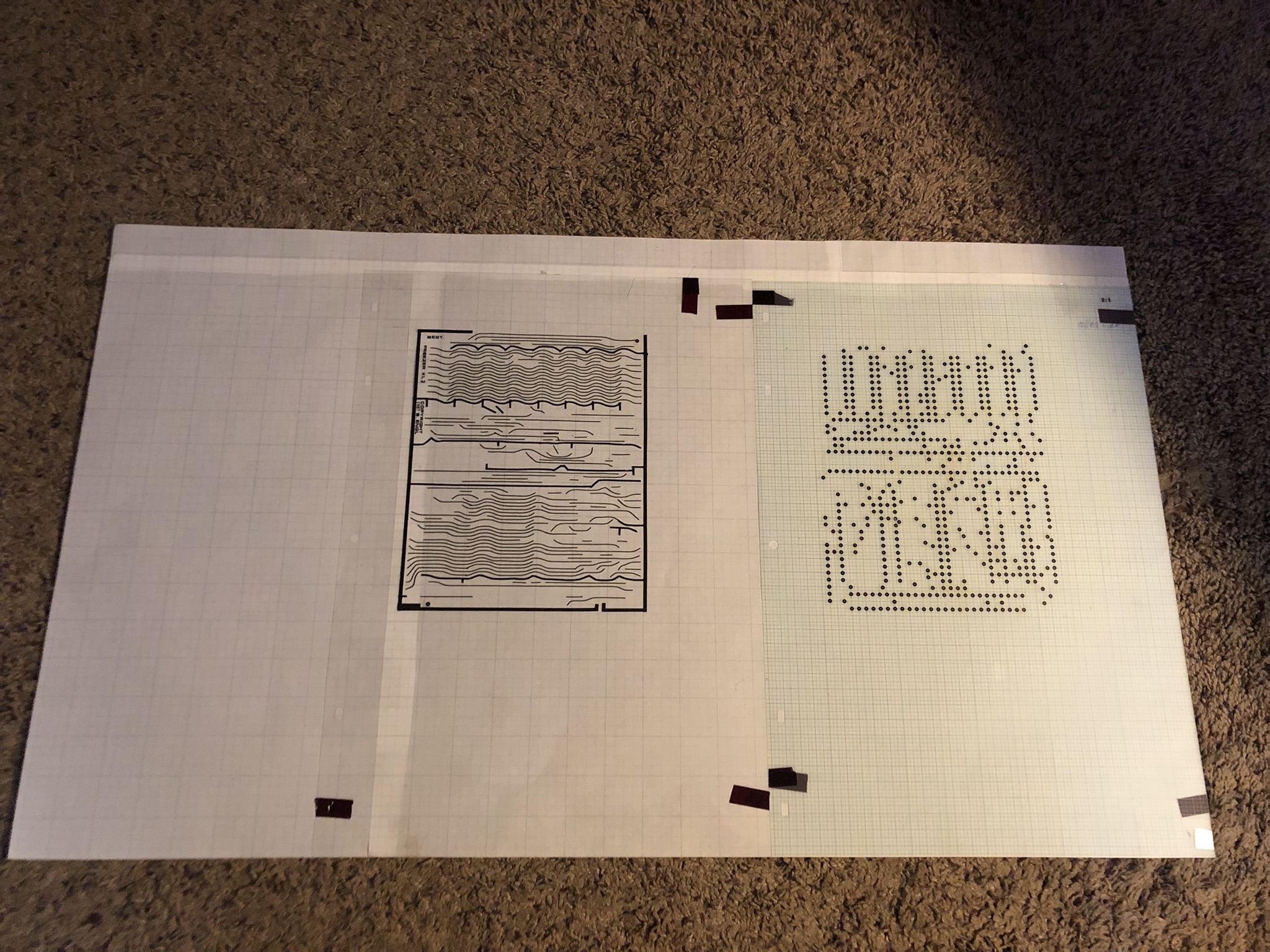
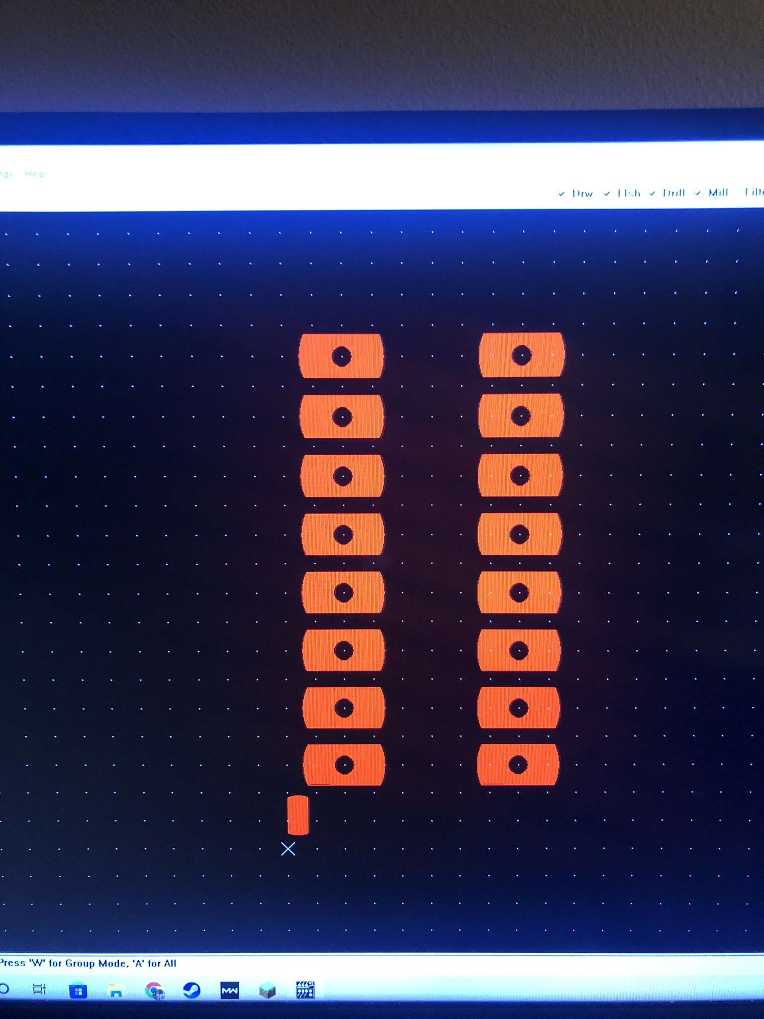
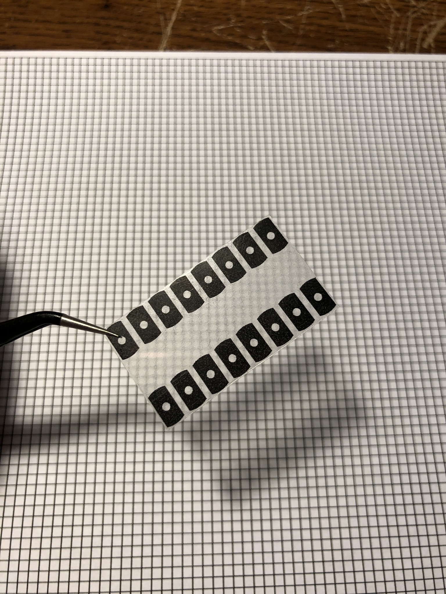
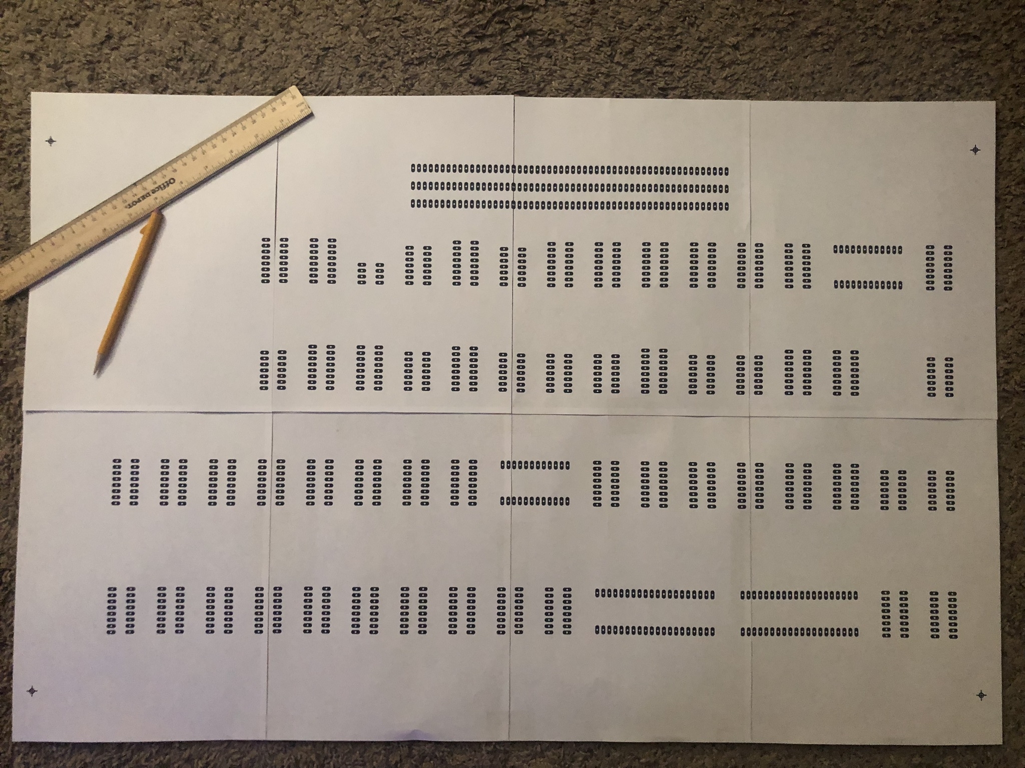
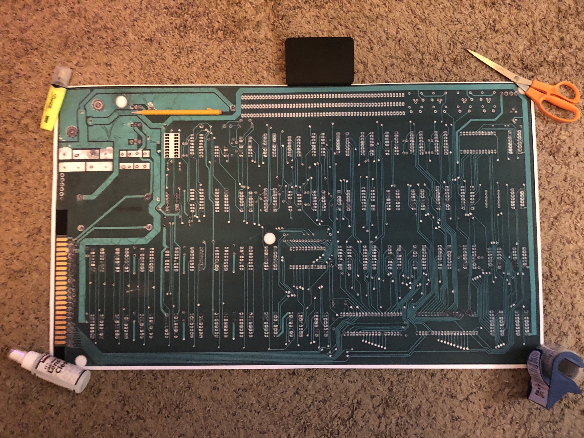
So, with all that in mind. As far as the projects progress goes over the past couple of months, I have been thinking in my head a lot about how to go about doing this. I started with the idea that the Apple-1 had to have definitely been 9X15.5 Inches, mainly because everything thats layed out on the board in the way it was, wouldnt really fit if it was any smaller, and would fit if it was bigger, but would mean that the board layout had to be enlarged beyond the REAL size. So, the way I figured this out is by the all drill holes and Pad shapes. So, the first thing I had to realize is that, I had to imagine myself in Howard Cantin's mind while I did this, the first step in starting the project is that I needed to get a grid, "Well, what kind of grid?", "What kind of size grid?", I studied through the Coombs book that ICs are designed to have .100' spacing inbetween every leg, NORMALLY, and so, I figured, if I had to physically draft the board, I would do it on this grid, but, what I found was that they don't make grids as large as I need. Remember, that back in those days, they would have had 4 common layout grid sizes for drafting, 1:1, 2:1, 4:1, 8:1. I knew that I couldn't lay the board out in 1:1 because my eyes are NOWHERE near as good to see everything, and so I ended up ruling to lay the board out in 2:1, which means that the finsihed drafting sheets would be 31X18 inches big, I'll discuss this a little later. So, with that in mind, I was also thinking about starting the drafting by doing the IC pads for the top and bottom side of the board first, and I think most of you guys are aware that the Apple-1s pads between the top and bottom, are different. I have attached photos of the shapes of those pads below. So, I had to figure out, what were the dimensions of these pads, there surely wouldn't be any recorded documentation about these, you'd be right and wrong. In my case, I got lucky in finding some actual 1:1 PCB drafting IC pad decals on fleebay. I have attached photos below as well.
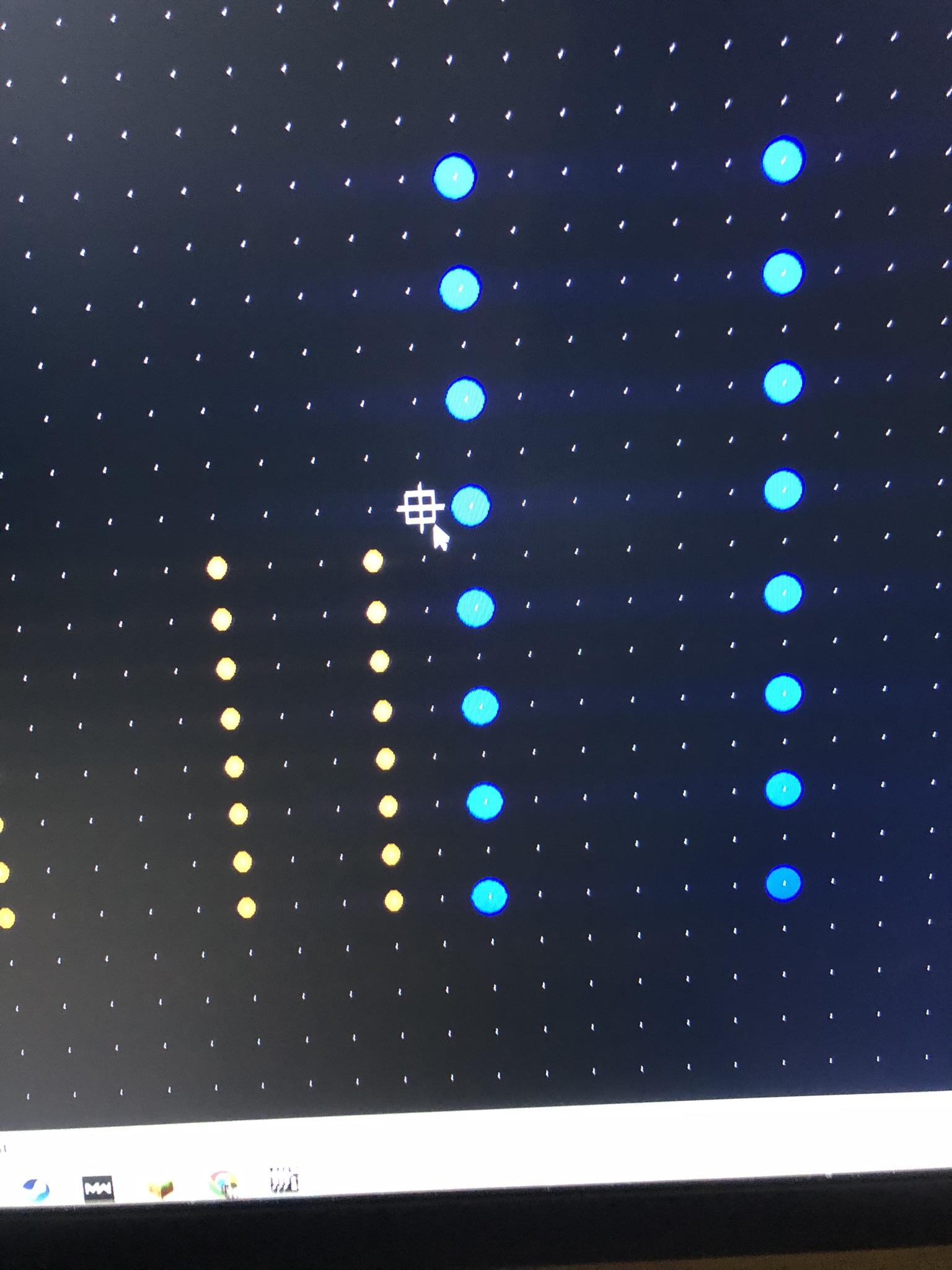
So, for the grid, I searched and searched for large TRANSPARENT 31x18+ .100' grids but just couldn't find anything. So, I decided, why not just create my own .100' grid in my CAD program, because my program can have a .100' grid, and so I loaded the grid, and then just started drawing very thin lines in the form of that grid size, then I made sure it was at MINIMUM 31x18 inches large, I actually made it 35X20 inches large, then now all I have to do is print it out on a large transparent sheet, which I am already doing as we speak. So, now I finally have my grid! Then I realized with those IC pads that they were made in 1:1, but they had all of the dimensions written on the packaging, so I just doubled each dimension, and then I had the right pad sizes for both shapes, WOOT! Now, I didn't want to buy 40+ year old decals that have super dryed up glue, they would be a waste of money and wouldn't stick well. So, again, I took by dimensions, and made all the IC pad shapes in CAD, to which they came out perfect. Then, in order to get the spacings in between each IC, I realized that if I scaled the whole Russian A1 gerber drill layer to double its size, the drill holes fit perfectly in my 2:1 pads, so then I just copied my pads across all the drill holes for ICs, and then I had my spacings perfect! I decided from then on that I would just place down in CAD, EVERY component hole in alignment with a grid, and I learned that Howard couldn't have just used a .100' grid, but he also had to have used .025', .050', .075, .078',& .100' grids at least. When I applied all these grids, 98% of all the component holes and pads, aligned PERFECTLY.
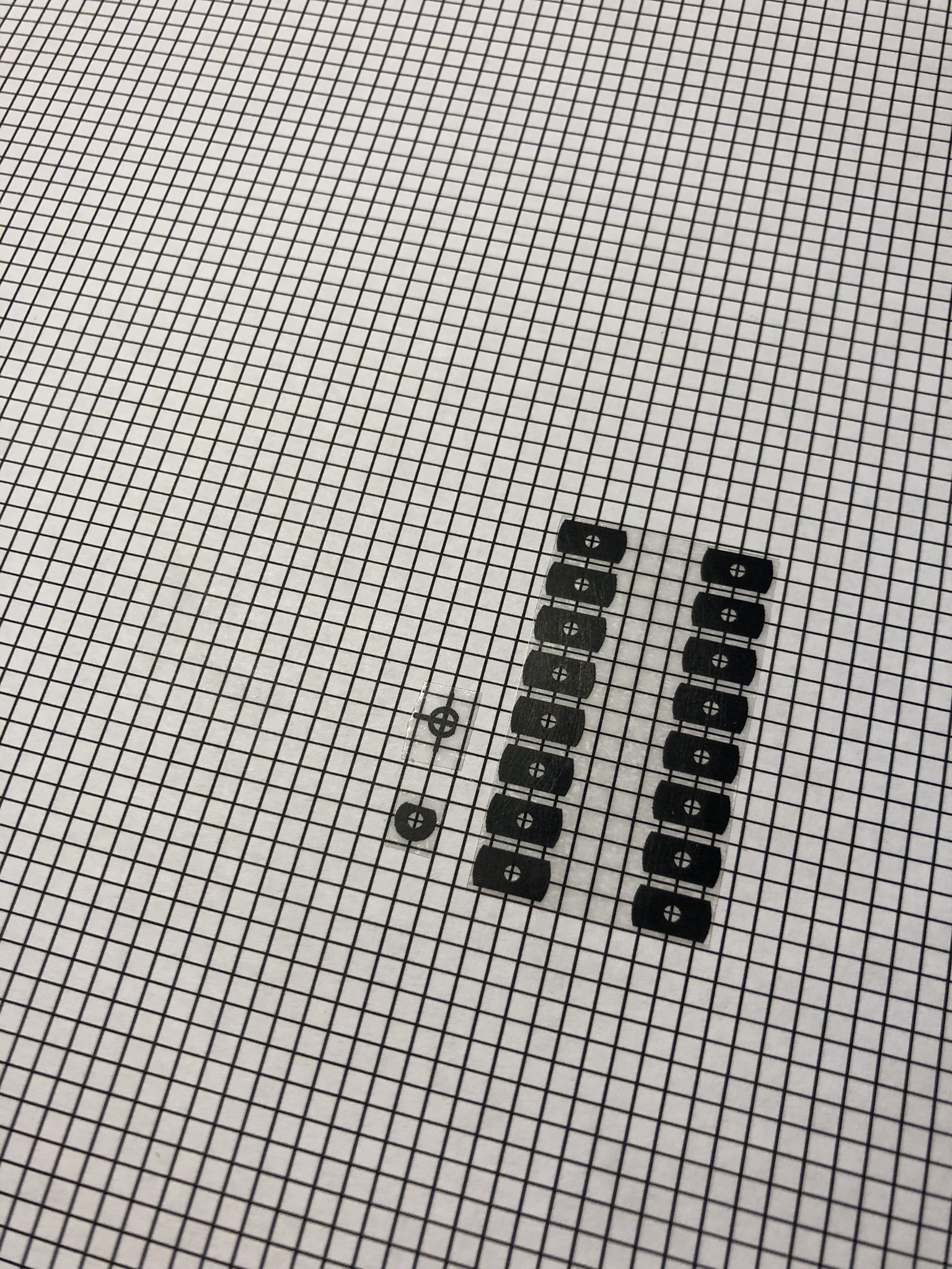
So, anyways, I now have all of my IC pads, and all other component holes layed down in CAD and aligned, I also attached one target marker in each corner of each layer so that way they can then be aligned later IRL. Then, I knew that all iI had to to then, is jsut either create of find actual drafting tapes, and then just print each layer I made in CAD on an individual transparent sheet of film. Then, to make my life a bit easier, I would just have to layout the actual traces with the tape, and that's what I am working towards right now. Also, theres a photo I published of me holding a transparent adhesive decal of back side IC pads adn I really loved that moment because I found transparent inkjet printable 8.5X11 sheets on amazon, and I then took my CAD pads and converted them to PDF, and then printed them, and that photo was how they came out and how easy they were to apply to things. Also, some of the photos I have attached are just of me printing and testing things to make sure all of my dimensions are right.
This is just about all I have on this project right now, but yeah, just thought I would share it with you guys.
All of this work is SO fascinating to me and really shows how much work really goes into a challenging project like this.
Enjoy the photos!!
Best,
Logan

As long as your replica motherboards are clearly marked as replicas then there should be no issues.