Hi
Just trying to get my head around how the PROMS are addressed in an A1
A0 to A7 are obvious. CE1 from B9 decoder as nCSF developed when A12 to A15 are high
Which gives the address range Fx00 to FxFF
But CE2 must be then low when A8 to A11 are high to give the address range FF00 to FFFF and I can't see how this is done. CE2 seems to be connected to B1 NAND gate with one input from the CPU clock and the other floating as the 6800 bits are missing ? Is it not decoded and always low meaning the PROM appears at multiple addresses ?
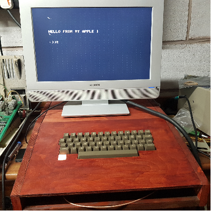
BTW, just got my A1 running with its keyboard tonight so ready to start playing.
Cheers for the kit UB :)
Well, answered my own question
Yes, the PROM exists in multiple 256 byte locations from F000 to FFFF.
Oops, you answered your own question before I could finish my writeup (or Ph.D. thesis) about the Apple-1 PROMs and how they are wired into the system. Of course, if you put a 256 Byte PROM into a 4 kByte address space without any attempt to decode it tighter, it will repeat 16 times.
But there is more to it, much more.
Many people have been scratching their head over the weird way the PROMs have been wired into the Apple-1. It's one of the worst mistakes in the whole machine. The NAND gate you mentioned (B-1, output #3) hopefully inverts the clock which goes into the PHI0 input of the 6502 (pin #37).
I say "hopefully" because the other input of the NAND is floating if the 7404 at C-1 is not populated (which it only is present in the 6800 case). Hoping that a floating TTL input produces a "H" is a practice every TTL databook warned about since the beginning of TTL. On most TTL gates it works OK if there is nothing connected to that floating pin. But if there is any kind of wire or PCB board trace connected to that pin which could pick up crosstalk, all bets are off. There is also a process technology related concern with leaking Schottky clamping diodes on LSTTL and STLL inputs, which could pull a feeble current out of the multiemitter input transistor, most likely not enough to be seen as a genuine low input level, but possibly interfering with the inner workings of the gate, such as reducing its noise immunity. Still, despite of all the warnings in the databooks, all too many TTL logic based designs of the 1970s ignored these helpful hints and so these neither are robust nor upwards compatible to 74C, 74HC and 74HCT families ... CMOS logic fails with floating inputs.
Why were these designers so lazy ? Well, the reason is that tying a TTL input directly to the +5V supply also is prohibited. A resistor is called for. Which costs money. And effort. And ink. And space on the drafting sheet for the schematics. Terrible ! So they let 'em float. Lousy designs these are.
But this is not all of the trouble with the firmware PROMs in the Apple-1. What this NAND gate produces, if it works despite of the floating input, is a signal that is low during the time the clock phase of the PHI0 (read: "PHI zero") clock input is high, which is similar to the PHI2 clock output being active H, but it's not the same. You can think of the PHI2 output of the 6502 being a delayed version of the PHI0 input.
We all know the 6502 fetches data during PHI2 being active H (the so-called "PHI2" clock phase). Hmmm. But an inverted PHI0 ain't no PHI2. The PHI2 is generated internally by the 6502, and all timing on the data bus refers to its falling edge, where setup and hold times have to be observed. The real PHI2 output was meant by the 6502 designers to be used as an enable signal for data on the data bus.
But in the Apple-1, both PHI1 and PHI2 made by the 6502 itself are ignored and substitutes with the same names are made from PHI0. Oops. Another foul ! The 6502 can have a T02- timing parameter of up to 65ns (for all speed grades up to 3 MHz !) which is the delay between the 6502's falling PHI0 input and the falling PHI2 output. Which is exactly the same PHI2 clock net internal to the 6502 dynamic two phase logic. It's brought out to a pin. No driver in between.
On read cycles, the 6502 expects a data hold time Thr of 10ns after the falling edge of PHI2. So, referred to PHI0, the data must be there on the data bus for at least 65ns + 10ns = 75ns measured from the falling edge of PHI0. Tell me how that is guaranteed in the Apple-1. (Hint: it is not). The only effect that rescues the whole system is capacitance on the data bus lines and the sluggishness of the NMOS 6502 to notice that its read data is falling apart / crumbling too soon. With CMOS 6502, which internally are faster, all bets are off.
This is another big, big design error which pervades the whole Apple-1 system. But everybody knows the old American adage: "What works, works !". Until it doesn't. This adage has been (and still is) a bane for American engineering throughout all industries. Only the Chinese are worse, they like to cut all corners and then some. The French like needless complications to show off how smart they are. The Italians are too lazy for that, la dolce vita is calling, so their designs are simple and robust, but their workmanship is questionable. The Brits have almost no industry left anyways. The Germans and the Japanese are perfectionists, overengineer everything and almost never meet time to market, the Japanese to a lesser degree. Korean engineering is a mix between Japanese and Chinese attitudes. The Americans do meet time to market, except in their MIC, but their products are as explained above. American cars being a prime example how not to build a car. Soviet Union engineering was driven by making designs as ugly as possible, and then get drunk. So each nation has its own engineering attitudes. Which shows. But back to the Apple-1.
Here is what could happen in the Apple-1: the NAND drives an active low chip select on the PROM's pin #14. PROMs, being bipolar, are fast to turn off their output drivers one the chip select rises H. So who keeps the data on the data bus stable after the PROM has turned its output drivers off too soon ? Before the PHI2 output of the 6502 has fallen ? Dirt effects do ! Good luck with that !
But, to quote Steve Jobs, "one more thing". The other chip select for the PROMs (on their pin #13) comes from the 74154 decoder. Note the absence of any use of the R/W signal in that signal path. So these poor PROMs don't know if it's a read or write cycle. And so, if you write to the PROM address space of the Apple-1 (a generous 4K for the 256 bytes of PROM), the 6502 and the PROMs have a bus contention and fight it out. Who wins ? Well, bipolar has very strong drive capability to low, and NMOS has only a weak drive capability to high. So at least in theory, the "0" bits in the PROMs should win. And of course, and hard work or fights with huffing and puffing leads to increased body temperature. You don't believe me ? Make a program that writes to the PROMs as often as possible, and then start it. Watch the 6502 and the PROM temperatures rise. But usually, no damage is done. But they get hot. Don't touch CERDIP PROMs being abused like that with your fingers.
So, we have three fouls / bugs / blunders in the design of the PROM interfacing in the Apple-1. It's no good. And would not survive any industial design review. But it has the advantage that it's so much against the rules for 6502 systems that everybody scratches his/her head how that thing works at all, so I can go ahead and write educated idle drivel.
How the hell could Woz put such a kludge into the Apple-1 ? I really would like to ask him, to find out if there was a good reason to do so. Maybe there was no reason and the Apple-1 really was a clean design for the 6800 and then later modified to accommodate the 6502, and possibly in a rush, just before the PCB was layouted.
In this light we can also see the allegations of the late Chuck Peddle who - shortly before his demise - has claimed in an interview which is somewhere on the web (audio recording, I have listened to it) that he, Chuck Peddle, toured the Silicon Valley area during that time, and he had the only in-circuit emulator for the 6502 family with him, to help customers with the design-in of the 6502 into their systems. Chuck claims that he also visited Woz to help him get the 6502 going in the computer which later became the Apple-1.
Alas, Chuck is not with us anymore, so he can't tell us what he saw on Woz' work bench (or kitchen table ?). Was it the hand-wired proof of concept computer, the one in the wooden box with open top you can find photos of on the web, or was it the first prototype on the PCB already ? Chuck got somewhat temperamental when he talked about Woz' skills as a digital designer, not very kind words, along the lines of "Woz had no clue", although not exactly these words, here my own memory is fading, too. The question is, no clue on what ? On the 6800 or the 6502 ? The standpoints of the two gentlemen may have been different !
As far as I am concerned, unless Woz speaks up and clarifies these allegations from Chuck Peddle, and tells us how everything really came into being, I can but take the tentative standpoint that Chuck in all likelyhood did not make this story up, so I think he indeed had visited Woz to help him getting the 6502 going in Woz' creation, and my conjecture is this may have lead to heated discussions about the way the PHI1 and PHI2 signals are created in Woz' design, which is outright wrong for a 6502 system, and leading to marginal reliability of operation. Some examples of the Apple-1 may have been more marginal than others, so your mileage may vary. But one thing is certain: when you start to violate datasheet specs, then the manufacturer of the IC will get angry if his Field Applications Engineers are called to the rescue.
And so, most likely, Chuck got angry and packed up his in-circuit emulator and left. Woz continued to generate PHI1 and PHI2 in the wrong way (for a 6502 based system). Which caused me a lot of grief, and weeks of debugging my floppy disk controller for the Apple-1. For the final "mass produced" version (pun intended, "mass produced" is a joke and may never happen due to lack of demand), I most likely need to create a local clock on the card, either with a PLL or an injection locked oscillator, or some other way, just to fix the timing, which is not robust at all (but right now at least on one machine it works well enough to develop the RWTS).
So far my conjectures about the 6800/6502/Woz/Chuck Peddle complex. If I would be forced to bet a reasonable small amount of money on how it really happend, I think it just may have been too late in the game for Woz to fix it after he got the lecture from Chuck. So most likely, they already had the PCB layout done, or at least in progress, or maybe they already had the prototype PCB in hand, when Chuck showed up to help. We know that the two Steves had gambled all their money on being able to series produce the Apple-1 for the BYTE SHOP order. So they may have decided to push forward despite of knowing that problem with the kludgy PHI1, PHI2 generation. I do know Woz' later design work very well and don't think he "had no clue", like Chuck has alleged. I think the two Steves just had to go forward to save their skin (which they had in the game). This is the most reasonable assumption. These things happen quite often in the industry and instead of fixing the issue that raised its ugly head late in the game, managers more often than not decide to release the faulty product and fix it later. So they reach their planned milestones, get the reward payments for being on time and on budget, and later they can blame the designers for being incompetent and being the culprit and responsible for all evil, and the millions spent later for the fixes and the product recalls never come out of the pockets of that manager.
Let me emphasize again, the above is just a hypothetical chain of events I made up based on the evidence at hand. But I have no other rational explanation why an obviously brilliant digital designer like Woz would make such mistakes in the Apple-1. I am inclined to think that the change from the 6800 to the 6502 came too late (the question that can't be answered is, when ?) to fully redesign the circuitry such that the 6502 is happy. As far as the 6800 goes, the Apple-1 design is flawless, except for the PROM data bus clash when writing to the PROM. For the 6502, the Apple-1 design is faulty. Draw your own conclusions which CPU may have been in the early handwired examples.
Comments invited !
Cheers
I have been scratching my head around that part of the circuit and the floating pin. I suppose its also likely it arose due to the change from 6800 to 6502 as the target CPU and maybe part of the intended DMA circuit ?
Its also why I wanted to build such a machine :)
Next to get my head around is why the A6 to A11 address lines can also carry A0 to A5, part maybe of an I/O scheme ?
Facinating.
Gary
Unfortunately, the PHI2 signal from the CPU is also ignored in the subsequent Apple II design. Not as bad as the Apple I but still caused issues for early Apple II expansion cards.
In post #5, jeffmazur wrote:
"Unfortunately, the PHI2 signal from the CPU is also ignored in the subsequent Apple II design."
Uncle Bernie answers:
Yes, I know. The Apple II inherited *a lot* of design ideas and techniques from the Apple-1. The keyboard codes. The monitor firmware. The cassette interface modulation method and the firmware. The expansion slot. The overall system concept: all on one motherboard.
And of course, the utter ignorance of the PHI1 and PHI2 offered by the 6502. Is this incompetence of Woz ? What do you think ?
A DIRTY LITTLE SECRET ABOUT THE 6502
Here is a dirty little secret for you all (if you are interested): a nasty pitfall awaits any designer who faithfully uses the 6502 PHI2 as suggested in the manufacturer's datasheets and application notes (originated at MOS Technology, and all second source manufacturers essentially copied it).
HOW THE 6502 PHI2 IS SUPPOSED TO BE USED AND HOW IT MAY NOT WORK !
It boils down to the suggestion that a combination of PHI2 from the CPU should be used to gate the read and write processes for all memories and peripherals. Unsuspecting designers followed that advice and in the 1970s it led to systems that worked. But beginning with the mid 1980s there were cases where it didn't work anymore, despite using the very same old NMOS 6502. This affected a product of mine which in the late 1980s caused a lot of phone calls and angry customers. I could only sell about a hundred or so until I had to stop production, scrap the rest of the PCBs, to design a new version that generated all the timing with an injection locked oscillator on that daugther card itself. Which then worked robustly and sold a tad below two thousand examples. Not with much profit, though, because I got screwed by usurers: the Signetics 82S105 FPLA suddenly was not available anymore (it had cost $3.50 or so) and the TI PLS105 at the time did cost 20 times that. Ouch ! Since then I hate those greedy IC brokers. They first sell you rare parts nobody else wants cheap and then when you start production and want more, they ask for moon prices. In the end I had to buy them from TI directly, but after a long lead time, and with the help of a friendly larger company. I think they might have started a production lot just for my order.
POST MORTEM - THE FATAL FLAW IN THE 6502
What had happened to me has happened to many other manufacturers of 6502 based computers or add-on cards for such systems and there was a lot of carnage. Essentially, it boils down to the 6502 bus timing design being botched. It has a fatal flaw which is well hidden in the datasheets, but it's there, in plain sight: Tadh (address hold time from falling edge of PHI2) is specified as 30ns minimum for the 1 Mhz and 2 Mhz versions, but only 15ns for the 3 Mhz version. This is from the April 1980 Syntertek 6502 datasheet. Maybe it was published on the 1st April 1980 ? Think about the reason for the 30ns to 15 ns shift for the faster speed grades. Which came from the same process in the same wafer fab. Can you see the problem ? Assume the process gets faster and faster. How can the 6502 manufacturer guarantee the address hold time ?
THE CHAIN OF EVENTS TO DISASTER
This is the chain of events which may lead to disaster: you combine PHI2 from the 6502 with some memory select signal from a decoder and R/!W from the 6502 to derive !RE and !WE signals for typical SRAMs. (I use ! as the inversion, and !RE and !WE mean active low read enable and write enable signals). This takes at least one LSTTL gate delay (~10ns). So from the rising edge of the !WE (which should terminate the write operation by closing the write gates within the SRAM) you have 5ns of address hold time left, until the addresses coming out of the 6502 may start to change.
Now, within the SRAM (from its !WE input pin) until all the internal write gates are closed, it may take more than 5ns, at least for typical, modern, mid 1980s SRAMs. So the write gates within the SRAM still will be open while the addresses start to change.
It now depends on the individual address decoder circuits within the SRAM whether this can occasionally corrupt some bits stored in the SRAM or not.
But it happend with some SRAMs from some manufacturers. The computer manufacturer having added additional driver gates for PHI2 contributed as it made matters worse by increasing the !WE turn off delay referred to 6502 PHI2.
IT'S NOT A BUG, IT WAS DESIGNED TO BE LIKE THAT !
Inspection of the 6502 transistor level circuit diagram - which I got decades later - confirmed that the addresses may start to change earlier than you would think. Maybe this lead to the demise of the NMOS 6502. If a manufacturer would shrink the masks to migrate the 6502 to a more modern process technology, they could not guarantee the datasheet address hold time anymore. And shrinking of die area was the number one trick in the semiconductor industry to stay competitive price wise. So the NMOS 6502 could not "follow the shrink path". Due to the way the bus timing was specified, they had shot themselves in their own foot. On the other hand, in the year 1975, who ever would have thought that a microprocessor designed in that year would still be in production 10 years (and more) later, using the same mask layout, with no changes, other than an optical shrink. They just did not think that the 6502 would last for so long on the market. (Think about Intel or AMD trying to sell you a CPU today, year 2022, which they already had in 2012 --- you would laugh your head off).
THE DEMISE OF THE NMOS 6502
If you were around microprocessors in the mid 1980s, you may have noticed that the NMOS 6502 suddenly got scarcer and the 65C02 popped up everywhere. My conjecture is that the CMOS version had a cleaner design as far as the address hold time was concerned, and it may have been designed with further mask shrinks in mind.
TECHNICAL PROGRESS IS NOT ALWAYS GOOD FOR PRODUCTS
So technical progress where improvements in process technologies yield faster transistors and faster ICs are not always beneficial. Some legacy designs can't be migrated and just stop working. So they disappear from the market.
In case of the SRAMs, they are a class of product any manufacturer must shrink aggressively throughout the life cycle to be able to compete price wise, and so the "same" SRAMs with the "same" type code got faster and faster, too, as a side effect, but not needed in the legacy systems that were still in production. I have seen humble 6116 SRAMs in the mid 1980s which were 5 x faster then the 200ns access time they were supposed to have. This high speed, of course, makes them more susceptible to changing address lines while the !WE is not yet gated off. The slow 6116 of the 1970s did not notice these crumbling addresses and so they worked fine.
THE REMEDIES
So you can see, even when using the 6502 PHI2 in the recommended way, you can end up with a wonky system. The best remedy is to use D-Latches on all address lines which work both as a tristate driver (to allow DMA) and to preserve the address for the memory well into the early PHI1 phase. The latch enable cannot be gated with anything combinatorially derived from PHI1 and PHI2, though ... to do this in a predictable way you need some sequential logic running off a faster clock.
This is a complete remedy for the address hold time issue. But for write cycles, you also have the data hold time issue. And this can be best avoided in write cycles by turning the !WE signal to the SRAMs off somewhat earlier than the falling edge of PHI2. However, for read cycles it's the opposite: turn the !RE signal off somewhat later than the falling edge of PHI2.
These remedies combined and skilfully tuned yield super robust system bus timing for any 6502 based system. But in the end it boils down to making "fake" PHI2 signals using a faster clock, and these "fake" PHI2 signals must have different turn off points for read and write cycles.
A SECOND LOOK AT THE APPLE-1 and APPLE II ignoring the PHI1, PHI2 offered by the 6502
Now, knowing that pitfall, and the remedies, and looking at the Apple-1 and Apple II design again, where Woz ignores the PHI1 and PHI2 signals from the 6502 and makes "fake" ones, we have to reconsider the allegation of incompetence. These fake PHI1 and PHI2 signals can help to get a more robust system bus timing ... write cycles definitely benefit from the PHI2 falling edge coming earlier than the same signal on the 6502. This shields the RAMs (or registers) being written to from crumbling addresses. But it worsens the data hold time issue in read cycles. Which was the issue with the botched PROM timing. But as far as the type 4096 and type 4027 DRAMs are concerned, this data hold time issue does not exist: they are able to present the data on their outputs for as long as you want, even after !RAS and !CAS have gone high. You just need to keep their !OE inputs active and the read data can get infinite hold time.
I think this feature of the early DRAMs is what may have rescued the whole Apple-1 and made it functional. The next generation of DRAMs (16k x 1), generic type 4116, does not have that feature, and so far this has thwarted my attempts to get a clean 20 kByte Apple-1 using these RAMs. Of course I do know solutions but all of them involve more mods to the basic Apple-1 DRAM control circuit than I want to do. BTW, all the 20 kByte and 32 kByte mods from back in the day for the Apple-1 are dubious at best, and for me they did not work. I do have a robustly working 20 kByte Apple-1 I use for my RWTS development work but it's using such a foul trick that I can't even tell you what it is ... it's the most rotten kludge ever seen in a microcomputer system since the infamous National Semiconductors IMP-16. But "What works, works !" (Old American adage).
Long post. But I hope it's enlightening for some readers and helps them to design, modify and build better 6502 based systems using fast modern ICs.
FIXING THE PROM DATA HOLD TIME PROBLEM
The PROM data hold timing problem can be easily fixed by cutting one trace at a nearly invisible point and then put in a short wire to ground the pin #14 chip selects of the PROMs. If you look on the solder side between the pin rows of PROM A1 there is only one long trace running between them, and at pin #14 of the PROM there is a little short stub (the stem of the "T") connecting the long trace to that pin #14, which actually goes to both PROMs, via another trace on the component side, it connects the pins #14 of A1 and A2. Obviously a good idea of the layouter (or Woz himself) to allow an easy layout mod: if that little stub is removed, and the pin #14 net is connected to address line A8, then you can drop industry standard 512x4 PROMs into these sockets. Which I have done in some of my machines to get twice the firmware space.
Note that the A1, A2 PROMs which come with my kits are a different story - these are 512x4 types, too, but no mod to the PCB is needed. With no mod, their A8 address line (on pin #14) stays connected to the "pseudo inverted PHI2" as before and on this lower page resides the Wozmon. In the upper page of my PROMs there is my famous diagnostics page which can be selected by slightly bending the pins #14 of both PROMs out (a ~25 degree angle typically is enough to prevent the pin from touching the contact in the socket). Then the A8 address line of these PROMs (which are TTL) floats and is interpreted as a logic "H" so the upper page with the diagnostics is selected. Oh, and the PROM data hold time issue also goes away in this case. So the diagnostics can run unimpaired in any case !
THE APPLE-1 IS A WONDERFUL QUIRKY FUN MACHINE !
There is a reason why I love the Apple-1 so much. It has so many lovely quirks that your "Uncle Bernie" has found a worthwhile candidate to test his digital logic debugging skills and instrumentation. And it keeps my mind busy ... nothing is worse than being retired and having no intellectual challenges anymore. I saw so many once brilliant designers turn into mumbling imbeciles within a few years after retirement. Just because they were too lazy to exercise their brain. And the human body is a marvel of thriftyness ... every organ that is not used or exercised enough, will shrink to the size that is juuuust enough to do whatever it is regularly being used for. This applies both to muscles and the brain. And possibly inner organs, like heart (a muscle), lungs, liver, kidneys, too. Use them or lose them. If you are a retiree, be warned !
Comments invited !
- Uncle Bernie
"THE APPLE-1 IS A WONDERFUL QUIRKY FUN MACHINE !"
Certainly is.
Mine is now running (from one of your kits) and running well. Just need to sort out the ACI as on the output the noise at the mid point of the voltage divider is greater than the signal.
Time to fit the reliability mods I think (even though it passes the PROM diagnostics for hours without an error)
In post #7, GaryC wrote
"Just need to sort out the ACI as on the output the noise at the mid point of the voltage divider is greater than the signal."
Uncle Bernie advises:
Oh, I know. Another lovely quirk of the Apple-1: more noise than signal ;-) on the TAPE OUT.
But this is a non-issue for most. The cassette recorder can't "see" the high frequency crap. And after a low pass filter the nicer and cleaner modulated signal emerges from the crap. Such a low pass filter is best hidden in the plug which plugs into the MIC input of the cassette recorder. If it's needed at all:
"Don't fix it if it ain't broke" (Old American adage)
Adding the "reliability mods" on the motherboard will not change the noise / crap level in the ACI daughter card in any significant way. And my "Gen2 improved ACI TAPE IN" circuit is robust against the crap. So I've postponed the experiments with the low pass filter in the plug until necessary.
- Uncle Bernie
Cheers
Wasn't sure if the noise was coming through from the 5v and as you have said, no advice without the mods :)
I normally use my PC as a 'recorder' and thats having none of it. I have seen your ACI mods and will look at them.