| Attachment | Size |
|---|---|
| 210.09 KB |
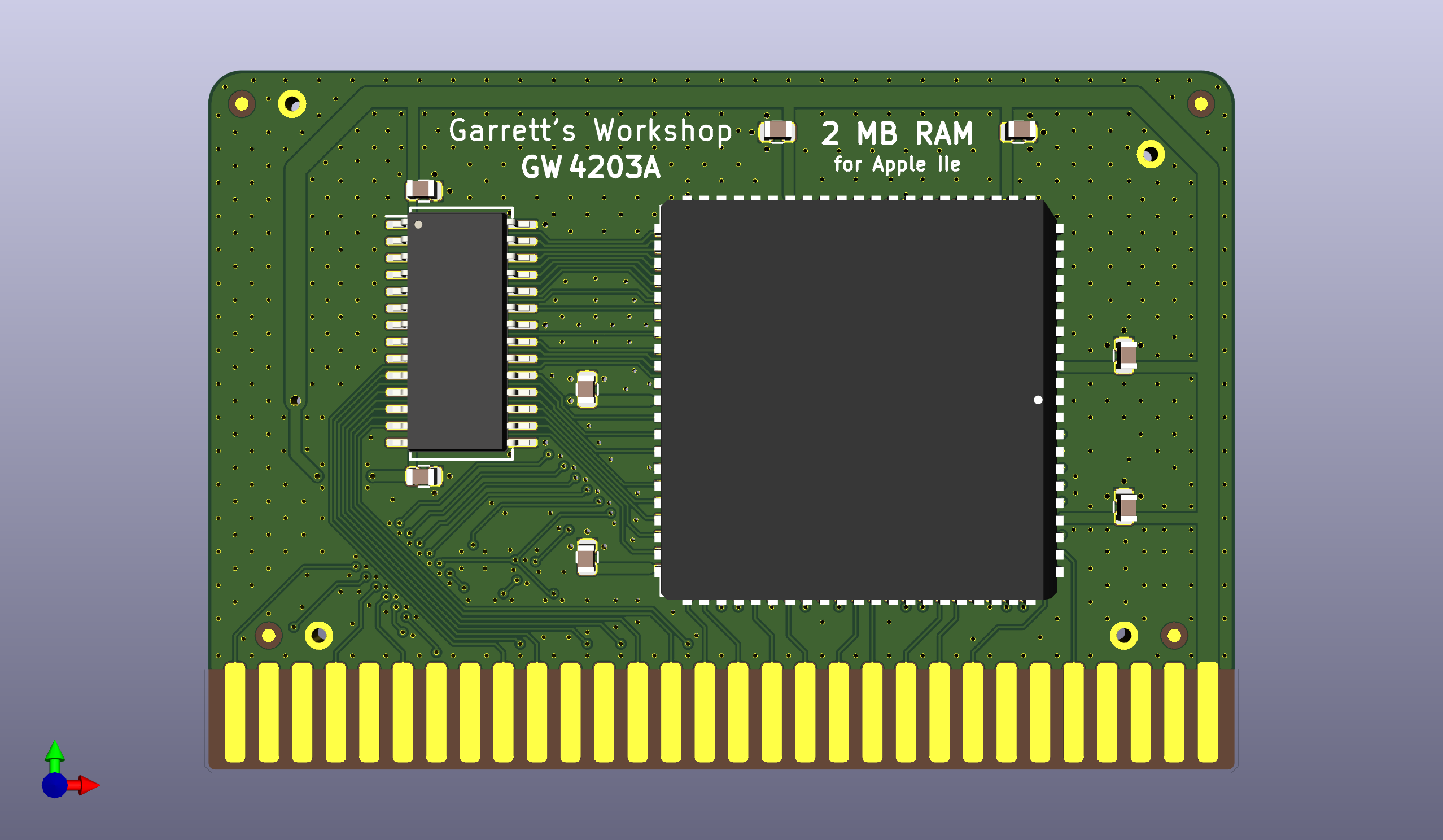
As mentioned in my "five new open-source Apple II cards" thread, my friend and I have developed some new Apple II card hardware, so the first one I figured I'd try to finish is the RAM2E (GW4203) for Apple IIe. This card goes in the auxillary slot and adds 2 megabytes of bank-switched RAM, switchable by writing the RAM bank address into the softswitch at C073.

The timing diagram merits a little explanation. The five signals on the top, below the C14M clock signal (PHI0, C7M, nPRAS, nPCAS, and Q3) are sent from the Apple II as inputs to the card. These signals in combination allow the particular state of the CPU/video cycle to be identified uniquely. There is no state counter. Instead there are some signals dictating what to do which are registered at the rising and falling edges of the 14 MHz clock: GateCRAS, nRefRAS, nRefCAS, GateWE, and HoldRow. Together these combinationally form the outputs to the DRAM: nRAS, nCAS, and nWE. This arrangement allows a CAS-before-RAS refresh cycle to occur prior to the video access portion of every 1 MHz cycle. The row address is latched on the falling edge of nPRAS as input from the IIe. Latching of the RAM bank address is accomplished at the rising edge of C14M in state 10100 (see the state bitvector definition in the timing diagram image) when the C07X signal is active and the latched row address (low-order address byte) is 0x73. The rest of the logic equations just implement the 74LS245 and 74LS373 on a typical extended 80-column card.
Of course, the schematic is attached. Since this card does not have software, we may refrain from releasing the board layout, at least not under the GPL... my feeling is that people should do their own board if they wanna sell it, but I would like to make the board layout available to people who want to acquire the parts and assemble their own. Or I could sell bare boards at cost. We will see what people want and probably just do that.
I have not yet compiled these logic equations in Altera Quartus II for the EPM7128 CPLD used on the board. Actually, I don't have a IIe, but I figured I could make a little contribution with this RAM board. So I will have to pick up a IIe soon to test the card with.
It has been some time, but I have 10 RAM2E cards in hand, ready for testing. I don't have a IIe, but I feel that I was pretty diligent in checking the final schematic, layout, logic design, etc.
That said, the timing diagram I gave in the previous post has a bit of an obvious mistake that made the whole scheme impossible hahah... So I have revised the logic design. All of the design files are available at https://github.com/ZaneKaminski/RAM2E and are licensed under a BSD-type license.
I will be reaching out to a few testers I have in mind to try out the RAM2E, and then I will fix any problems, do a second round of testing, and then release of the card.
Zane,
I have a rev B //e and 3 Platinum //e.
[quote=Zane Kaminski]
It has been some time, but I have 10 RAM2E cards in hand, ready for testing. I don't have a IIe, but I feel that I was pretty diligent in checking the final schematic, layout, logic design, etc.
<< SNIP >>
I will be reaching out to a few testers I have in mind to try out the RAM2E, and then I will fix any problems, do a second round of testing, and then release of the card.
[/quote]
You need to get a ][e....
Virtual Hardware is difficult to Trouble Shoot...
MarkO
Done!
igNa0gwdTlSwFZlDlhuXrg_thumb_23c5.jpg
Now I've just gotta fix it... But it did come with some good cards, notably an Echo+ speech/sound card.
So it should be easy to finish the RAM2E soon and get it released. My slot 1-7 cards are suffering from some compatibility issues with other cards, so they are sort of delayed until I can figure that out. RAM2E is easier to ensure it works since it doesn't share a bus with a bunch of other cards.
Bus timing issues with slot 1-7 cards can be tricky, especially if you are using CPLD/FPGA parts instead of old school 74 series or CMOS parts or GALs. Even GALs have their own things to consider.