Hey
I am new to this forum and I received an Apple iie a while back, but just now stated to repair it.
I have this board and the manual. I was wondering if someone had more info I was looking for a copy of the disk and maybe the pinouts so I could make the cable.
A better resolution photo woould be nice.... hard to make out whats there. It appears to be a parallel card... some of the early ones have odd pinouts though...
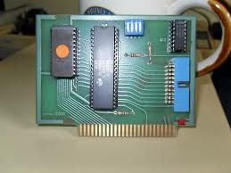
I agree with Spectre. It does look like a parallel card. The big 40 pin chip is likely a 6521 or 6522. The 24 pin chip is obviously an EPROM and the other smaller chip is probably something like a 74LS245 or a DP8304. That's a pretty simple and common parallel interface design. Usually the pinout to the IDC30 connector is a fairly simple mapping to a Centronics style printer interface. The DIP switches are usually to select the exact configuration of some of the signal pins or to select parts of the EPROM to be active for things like different printer configurations.
This type of card can be a lot of fun if you know what the pinout of the connector is and how to program to it directly as you can often do similar things to it as the GPIO pins on modern microcontrollers like Arduinos or the Raspberry PI. It's usually even possible to interface to devices like that with this kind of card.
WP_20200308_12_13_45_Pro.jpg
It's definitely a parallel interface. The 6522 is totally expected. I would be interesting to see the back side of the board to see how the CD4050 is hooked up. I would have expected a different chip but it isn't completely different than the 74LS245 or DP8304, probably used for a similar purpose.
It should be possible to figure out what the output looks like based on what pins of the 6522 connect to the output.
A dump and disassembly of the EPROM contents would also be extremely interesting.
Might be of interest --
https://groups.google.com/forum/#!msg/comp.sys.apple2/XHuGKArVk28/vW1YL1T6AKoJ
I'm thinking not: the major difference is that the '248 and DP8304 can tristate their output pins.
The CD4050B is just a buffer (non-inverting, in this case) with no tri-state ability. It does, however, do logic level conversion: according to the datasheet, "the input-signal high level can exceed the Vcc supply voltage when these devices are used in logic level conversions."
So my guess is that this would be used to protect the input pins (or, for you hackers out there, those pins usually used for input in a parallel printer interface) from overvoltage inputs.
(I am pretty sure this isn't used for the outputs because a) there are only six buffers in that chip, but at least nine output lines, and b) if you need outputs driving higher than TTL level you can use PIA port B, which has internal pullups. At least, I think port B does on the 6522; it's not totally clear to me from the data sheet if it's the same as the 6821 in this respect.)
That said, take this all with a grain of salt. I am not an expert, I've just picked up some bits of knowledge about this recently while adding a second 6821 to my Apple I replica SBC.
That's an interesting theory cjs. Makes me more curious to see the other side of the board to see what that CD4050B is doing. It isn't usual to see an Apple II board with a 2716 that doesn't have some decode logic, so I am assuming maybe the dip switch is hard-coding it into 256 byte chunks into the default card space. It also isn't usual to see a 6522 without a 74LS245 or DP8304, so I'd be interested to see how it is wired. Perhaps they've hard wired the 6522 for a very simple case of parallel out on a single 8 bit port and it doesn't need anything else.
Sorry for not quoting in a better way, but this board software ...
You can have a 2716 without adding logic elements. Write the code from $0100 to $01FF for slot 1, from $0200 to $02FF for slot 2 ... or write code for every slot to $0000 to $00FF.
It's also ok to have a single 6522 without any bus drivers. But it's necessary to avoid timing problems with the /CS and the clock, see the official Apple paper:
Tech Info Library
So I think that this CD4050 has also a similiar function: delay of the clock signal. This was a common method for example look at this board:
2* VIA6522
Regards
Ralf
Ah, yes! RalfK is correct; I'd forgotten that the clock signal needs to be delayed, and the 4050 may well be doing that.
Decoding for each slot is done on the motherboard, as described starting on page 80 of the Apple II Reference Manual, so there's normally no need for decoding on the card:
Really? What would a tristate buffer be needed for? Not between the chip and the bus, since the chip has device select pins to take it off the bus. On my board the 6821 is just wired directly to the bus with a bit of logic to enable the chip when the I/O addesses are selected.
Yes, that would be my guess; it's a pretty standard way of doing it.