
I'm working on a board to add a -5v signal to an ATX power supply, so it can be used to power an Apple II. The design is based on SpeedyG's, but I wanted something I could just plug an ATX power supply into, rather than cutting it up. I've always wirewrapped or breadboarded, but I wanted to do a proper PCB, now that they're so easy and cheap. This is my first time using KiCad, first time doing a PCB layout, and I don't have any background in analog circuits, so I was hoping I could get some advice on the design.
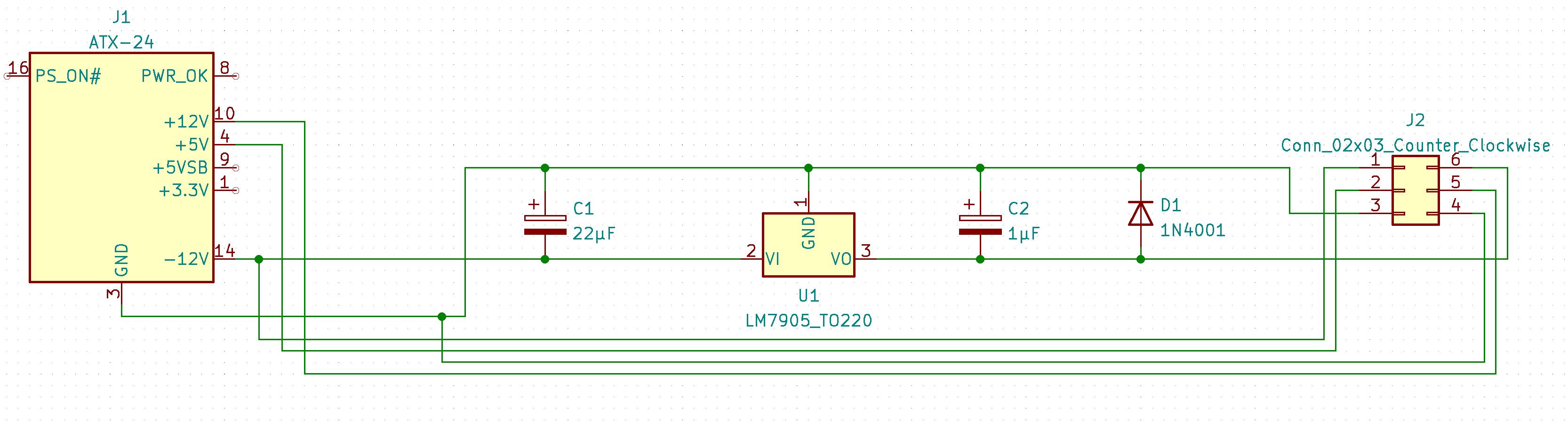
This is the schematic, which is just a copy of SpeedyG's with the connectors added in:
This is what I have so far for the PCB:

If you spot any problems, I'd appreciate hearing. I also have some specific questions:
The Apple II power supply is rated for 4A at 5V. I made the power traces 2.7mm to match the pads. It looks like that gets me almost what I'd need for a 5A rating. Seem reasonable?
By default, KiCad wants to route these traces awfully close. My understanding is that the space between traces should be about equal to the width of the trace. Is that a reasonable rule of thumb for a design like this?
Can I get away with putting power traces at the same location on opposite side of the board? For example, if I ran that ground line at the bottom on the opposite side of the 5v line. If I space everything out the way I think it should be done, the board gets awfully big for what it is.
The area around the capacitors seems sloppy and too tight. Should I space that out more?
I see nothing wrong with your design (although you could update the schematic to show your new pin numbers). And you definitely can run traces on both sides of the board, even making them "power planes" if you like (although not really necessary here). The -12 trace could also be made smaller if you need to.
Looks nice. A few years ago somebody sold something similar to that which worked with Micro-ITX power supplies ,some of which are small enough to fit into a ][+ or //e case, but I haven't seen them offered recently.
I suggest that you move the traces apart so that they don't come so close to the via's and solder points. Leave adequate space between the traces as well.
It doesn't take much but it looks like they are barely separated. Referencing the trace image, it looks like you've got the space available to spread the trace a bit.
The WIDTH of the trace you are using is plenty good and can actually be a little less if you lay down a heavier copper trace. (or double up as previously suggested) Your choice on that.
How's this?
Screen Shot 2022-01-18 at 11.53.47 PM.png
Well done!
A bit cleaner, now. This is addictive!
(The hashed area is supposed to be a solid fill to act as a heat sink, but it's not showing up in the 3d view, so I don't think I have it quite right yet.)
Screen Shot 2022-01-19 at 1.40.22 AM.png
... Add a 45 Deg angle to the RED trace at the top-right of D1. All other traces have 45's to them, this one doesn't. ;-)
Function-wise, it makes zero difference. It's pure asthetics. Nice work BTW.