| Attachment | Size |
|---|---|
| 238.38 KB |
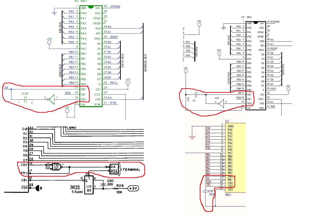
I'm trying to figure out whats the purpose of a NOT gate that's connected on pin CB2 of the 6821. In Tom Owad schematic this gate is connected to pin CB2 and then coupled with a capacitor to pin PB7 which is DA. To me this is useless because the cap will filter the output of the gate. On Briel's schematic the output of the gate is directly connected to the DA signal which I'm guessing both CB2 and DA are outputs and may probably create a logic contention. In the R1 plus the gate disapeared and instead there is capacitor connected from CB2 to ground. The original schematic is more similar to Briel's schematic but it shows that CB2 is an output and PB7 is an input which makes more sense.
Hello reb2015,
welcome to the board....
the signal at CB2 is used to control the B Port and the gate causes a delay....
in general such a delay is used to delay the time when the chip will accept
the data at Port B to contain valid Data.
speedyG
It might also help to understand how port B is being used on the Apple 1. It is connected to the display logic and is used to handshake the data being output. From the Apple 1 ROM:
The data port is being used as both input on bit 7 (terminal output ready to accept data) and the character data on bits 0-6.
NOTE: this code is backwards from section III of the Apple 1 Operations Manual (BPL vs BMI).
It could be that Woz didn't have this NOT gate there originally to bit 7. That might explain why there is a discrepancy between the actual ROM code and the description in the manual. It doesn't appear there is an logical benefit to inverting the signal on bit 7 of the data port (DA to the terminal appears to want it inverted). Maybe it was one of those "Woz-isms". And adding the cap could also delay/clean up the reading of the the DA value.
Dave...
I'm sure someone can correct me if I'm wrong, but this is my understanding:
wozmon writes
$A7to PIA CR A and CR B, so the CA2 (unused) and CB2 lines are configured as outputs (CRx[5:3] = 100 binary). The description of this configuration for CRB (CA2 is similar, but designed for a read access) is as follows:So CB2 goes low upon a write of a character to PRB, and this needs to be inverted because the DA input to the terminal section (C7 pin 4) is active high (the bubble on the connection to the terminal shown in the processor section seems to be a mistake?).
The terminal section brings /RDA low when the character is consumed (DA && CURS at C6), and the falling edge triggers the one-shot (B3) to generate a negative pulse on its /Q output attached to CB1.
The CA1 and CB1 interrupt inputs are configured (CRx[1:0] = 11 binary) to set the interrupt flag bit on a rising edge of the input. Thus, the positive edge of the low pulse causes the interrupt flag CRB-7 to be set to 1 after some delay, which in turn causes the CB2 output to go high and de-assert DA to the terminal section (and PB7).