
While exchanging on some problems that I am facing on building a replica, I realize something that is probably obvious for most of you, but was not for me.
I have been working the last few years on repairing Macintosh computers, most of them being multi layers mother board.
I realize that Apple-1 board is 2 layers, top and bottom. So, I should be able to see all the traces on the board.
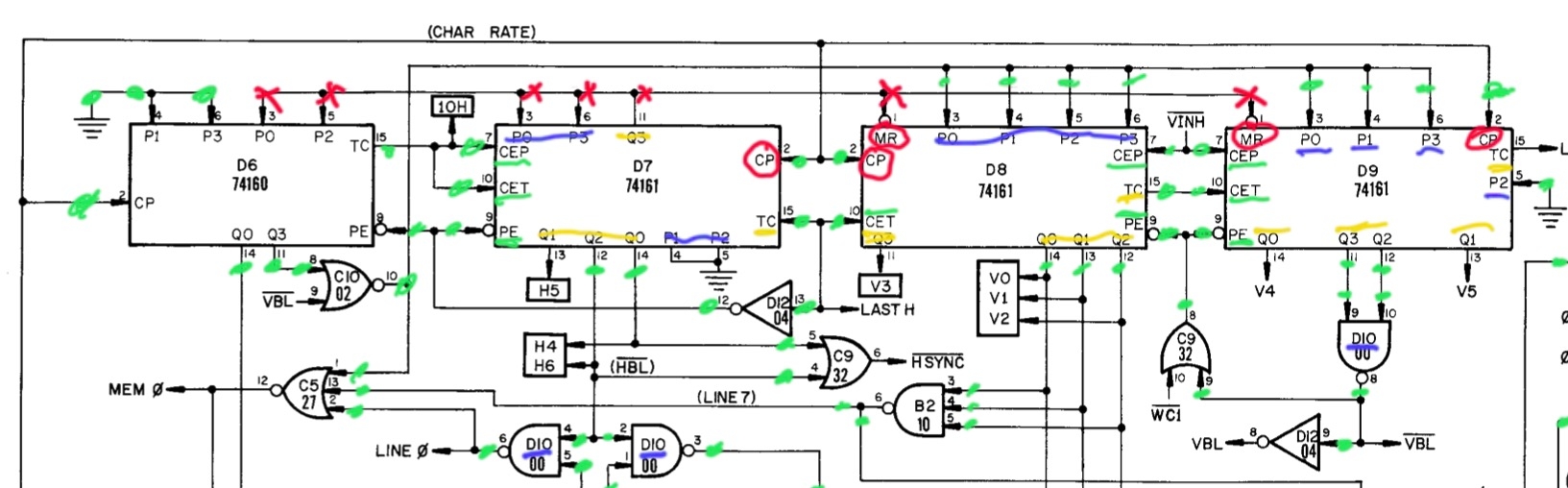
Could someone check on his board if they have a trace or connection on the pins marked with a red cross on this schematic?
On my board, I do not have any connection and no trace is coming to these pins.
I think Mike Willegal reported that https://www.willegal.net/appleii/apple1-hardware.htm first.
Check my post here for a better diagram:https://www.applefritter.com/comment/113096#comment-113096
In short it does not make sense, it's simply bad design.
In post #3, 'natas666' wrote:
" In short it does not make sense, it's simply bad design. "
Uncle Bernie comments:
Leaving TTL inputs open ("floating") to get a "H" level on them was a common practice since TTL was invented in Y1963. Except it was not called "TTL" yet, they called it "SUHL" when the first of them became available in Y1964. They were too expensive anyways back then, at least for civilian applications. Other logic ICs like Fairchild DTL were cheaper.
About a decade later, Texas Instruments ("TI") started to warn about the practice in their databooks. Woz might not have had the newest databooks when he designed the Apple-1.
Now, if you look at the transistor level circuit of typical TTLs, you will understand that the "floating inputs" indeed give a reliable "H" level EXCEPT when they could pick up crosstalk or suffer leakage current to ground, the latter of which is rare except for very harsh environments where the circuit boards are exposed to dirt and humidity. Crosstalk pickup is only possible when long PCB traces are attached to such input pins and then left floating. Capacitive coupling would then cause problems. This may have been the reason why this long "H" level line in the Apple-1 schematic is not present on the PCB layout.
TI also did warn against tying "H" level input directly to VCC (+5V). IMHO this warning is over cautious, you can always safely tie a TTL input to to the VCC pin of the same IC package (there is simply no way this could ever allow a parasitic diode to open). But there is a danger if a TTL input is tied to a VCC source NOT on the same VCC net as the IC having that input. Then, a current limiting resistor as advised by TI is necessary to prevent blown up ICs. This danger is present when a PCB has multiple 5V regulator ICs ... which sometimes was done due to the output current limitations of these regulators.
None of this applies to the Apple-1.
So, is it a "bad design" ?
No, it isn't, as far as the circuit design of the motherboard is concerned. All the problems with reliability / random program crashes come from poor PCB layout ... too narrow VCC and GND traces and Schottky TTL driven multiplexed address lines being too long and branching and having no termination resistors are subject to ringing and this wrecks reliability. Too few power supply bypass capacitors also play a role ... but was this Woz' fault ? At the time the Apple-1 was designed, the DRAM manufacturers were lying about the huge current spikes their DRAMs generated (lying by omission). Only when they found out that nobody would want to use DRAMs because their prototypes did not work reliably, the DRAM manufacturers admitted the problem and provided remedial guidance on how to do the layout and the bypass capacitors. They even showed the huge supply current spikes (> 100mA per DRAM !) triggered by RAS and CAS strobes in their app notes or even the datasheet. And from that point in time on, DRAM was successfully adopted in more and more microcomputer systems, and SRAM disappeared in these applications ... too expensive per bit compared to DRAM.
My "reliability mods" which I published here in Applefritter many years ago bring remedy to all these problems and the Apple-1 with these mods work 100% reliably, as long as the ICs are not defective.
The ACI ("Apple Cassette Interface") was a botched design however. Obviously, as brilliant Woz was as a digital designer, as helpless he was as an analog designer. I also fixed it, but this requires major changes to the comparator circuit and the PCB layout.
What to do with the "Bugs" in the Apple-1 schematics ?
I had a discussion with Armin about this topic and suggested he should revise the schematics in his Apple-1 manual reproductions so as to fix the errors seen in the originals. But his point was that this would destroy the faithfulness of these reproductions. Opinions on this topic of faithfullness and exactness of reproductions of course will differ, depending on whether you are more of an engineer or more of a collector.
- Uncle Bernie
@UncleBernie
thanks for the explaination and especially the historic point of view.
I already heared that the 74 TTL-Chips without letters have been far less sensitive to floating inputs but it was new to me that it was considered as safe at least for some time.
Looking at the schematics again the error is also in redrawn schematic you find on Hans Ottens page and on the KiCAD version I linked to here: https://www.applefritter.com/comment/113096#comment-113096
All the bussed inputs are connected to one output of Q3 of IC D7 while input D3 is one of the bussed together inputs.
That does not look good to me for three reasons: 6 inputs are connected to one output, Input D3 and output Q3 form a feedback loop, Q3 is pulsing as D7 is a 74161 binary counter.
So the connection to IC D7 Q3 needs to be removed and instead all inputs tied high.
On TTL prices, I remember the headlines in the European Mullard Bulletin (a trade paper from that manufacturer). It was "TTL down in price to ten shillings a gate" - this was late 60s or early 70s. That is 2 GBP for a 7400. The Bank Of England inflation calculator makes that around 30 USD in today's money.