
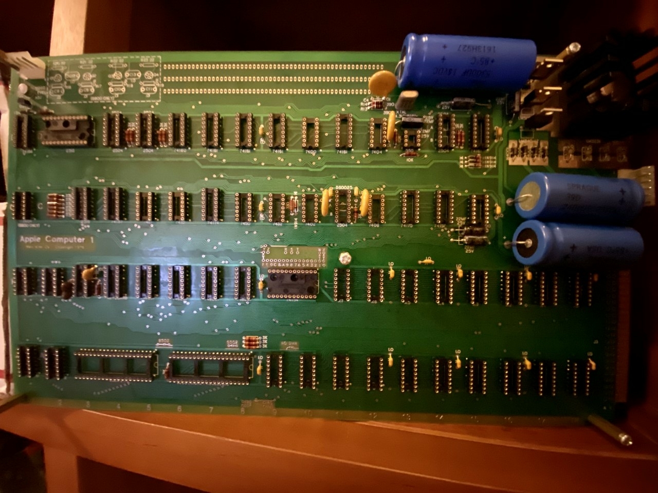
After a lot of work I've got this far with my Apple 1 Mimeo build.
I'll be putting together my PEM this week, any wisdom or tips for somebody at this point in a build?
If you could go back in time what would you say to yourself when you got to this point?
thanks,
Juan
I'll repeat what I put in my build manual. "Instructions can be found in the Apple Operations Manual that can be downloaded from many websites, such as http://www.applefritter.com. The only recommendation beyond what is in the manual, is that both fuse and switch should go on the “hot” side of the 110V AC input. I strongly recommend that the transformer and 110V AC wiring be placed in some kind of well ventilated enclosure. This is to make sure that no stray body parts touches any part of the 110V AC wiring. It must be well ventilated or fire could result from excessive heat build up."
Furthermore, I recommend that the power switch is first and the fuse second, so if the switch is off, the fuse is NOT energized.
Here is how the enclosure for my power supply looks.
http://www.willegal.net/blog/?p=893
regards,
Mike Willegal
I'd also put a 1 Meg Ohm bleeder on the power supply... Search here there are some threads on it.
Cheers,
Corey
Juan -
nice build, congrats !
Here is my 10 cent of advice: put a 100nF ceramic bypass capacitor between -5V/GND and +12/GND on every other DRAM on the PCB backside. Each DRAM gets one cap which fits nicely. I did use a pattern like:
A B A B A B A B (upper row)
B A B A B A B A (lower row)
A is for the -5V/GND bypass, B for the +12V/GND bypass. This pattern was recommended in a vintage Intel datasheet for their 4k x 1 DRAMs. They really urge the reader to put these bypass caps in and even show the fierce current spikes produced by the DRAMs. There is no way to get that current pulses over the pathetic power supply grid of the original Apple I design.
You may also add two 100nf bypass caps between +5V/GND on the center DRAMs.
My build did not work properly and had lots of memory test fails before I put those caps in. Lazy as I am, I first tried to get away with just a few caps as posted by others elsewhere in this forum but this only improved things so much ... one DRAM fail per day instead of one per hour. Now with all the caps in as described above, I can run Mike Willegal's DRAM test for weeks with zero failures. Disclaimer: I use the DS0026 clock driver and not the DS0025 which is much more benign. This is why some Apple I may work (almost ?) even without adding that elaborate bypass cap bank, but I doubt that any of them ever was truly robust as far as DRAM reliability goes. There is a reason why Apple "bought them back" by swapping them for a discount on the brand new Apple II. Some stories by insiders published on the web state that Woz himself had to take the customer support calls for the Apple I which blocked him out and kept him from working on the Apple II. So they decided to thin the herd (of Apple I in the wild) to take that pressure off Woz. The root cause why there are so few original Apple I left.
The deeper reason for all this trouble is twofold: a) DRAMs really need good local bypassing to mitigate their own current spikes and b) the PMOS shift registers driven by the DS0025/0026 couple their clocks into their -5V supply line which pollutes it badly. The DS0026 makes faster clock edges so the problem only gets worse. I think the two Steves in their garage just got "lucky" enough to have ran into a DS0025/Shift Register/DRAM combination where the problem did not manifest too badly, so they could sell their product, despite of that deadly flaw. We don't have access to the same parts from the same manufacturing lots so for us all bets are off, unless we put those extra bypass caps in. I am quite amused about the speculations you can find here and elsewhere about which are the "good" parts that will work. There are no "good" or "bad" ICs or "good" or "bad" IC manufacturers. Just an utter lack of proper power supply bypassing in the original Apple I PCB.
But this was a common problem with many hobby / home computer designs back in the 1970s. I am also building an OSI Superboard II clone now - its power supply PCB layout is pathetic, too. Back in the day, you could also buy S100 DRAM cards that almost worked ... but never worked well enough to use the machine other than as a toy. There is a reason why most of those pioneer companies disappeared as quickly as they popped up... Apple just got the corner without flying off that cliff, but IMHO the tires were screeching and they just barely survived it.
Bernie
PEMv1.jpg
Thi s is my initial PEM. I've not yet plugged it in to test the board (without ICs) as I want to be sure it's wired up correctly.
I was wondering:
What voltages would you expect for P1 to P6 without a load?
Why does the instructions say right and left wire for the output wiring? That is annoying me as right and left is dependent on which way you are looking at the Transformer and I am not certain I have put P1 & P2 ot P3 & P4 in the correct orientation. I don't want to mix that up, plug into my mainboard and blow it up :(
Anyway, I'm getting some more heat shrinking today to tidy it up. It's a long weekend in Singapore so I may have enough time to test this out.
cheers,
juan
thumbnail_IMG_1499.jpg
Got to drop it down to 110V before I go to the transformer - what with me being in Singapore and all. I think 500 Watts is overkill though.
Nice that you have it. Maybe a bit overkill, but not too bad. Better overkill than underkill.
Nice looking converter.