| Attachment | Size |
|---|---|
| 2.83 MB | |
| 3.82 MB | |
| 3.74 MB | |
| 3.71 MB | |
| 393.38 KB | |
| 135.14 KB | |
| 64.63 KB | |
| 1.6 MB | |
| 77.69 KB | |
| 358.95 KB | |
| 854.35 KB | |
| 3.86 MB | |
| 3.8 MB | |
| 3.53 MB | |
| 3.85 MB | |
| 3.65 MB | |
| 3.94 MB | |
| 3.85 MB |
Greetings. If you've been following my previous thread (Apple II Plus Bad Memory/ROM? - The saga continues), you'll recall that I recently purchased an Apple II Plus motherboard with the intention of using it to replace the faulty motherboard I already had. Unfortunately, it turned out that the eBay motherboard was even less functional than the one I already had. I was ultimately able to get the original board working by swapping a few chips from the eBay board, and I now have a fully-functional II Plus.
Now, I am trying to see if I can repair the motherboard I received from eBay. The seller claimed it was a working pull, and I have no reason to assume they were lying; it is entirely possible that it did indeed work when they packed it up, but then something happened in-transit to damage it. It was wrapped in bubble wrap with no other anti-static packing material, so it is possible static got it, or rough handling. It's hard to say.
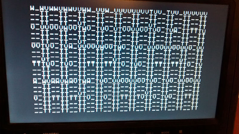
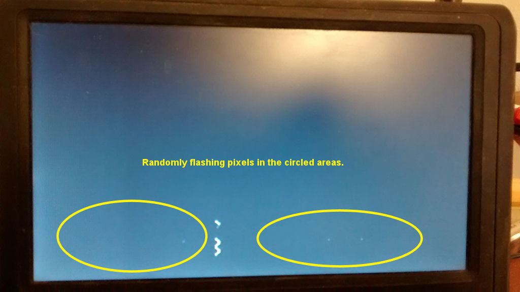
When the board is powered on, the power light does turn on, but there is no beep, and the screen either shows nothing at all (The TV I'm using for a monitor simply says "No Signal"), or it shows random garbage, as seen below:

This occurs regardless of whether the disk controller card is installed or not. When it is installed, there is no disk activity at power on. The board arrived missing the 9334 chip at F14, but swapping in the 9334 from my working motherboard doesn't make any difference. I learned by accident that my working board will still boot without a 9334 chip (It just won't display "Apple II" at power on), so I presume the same should apply to the faulty board.
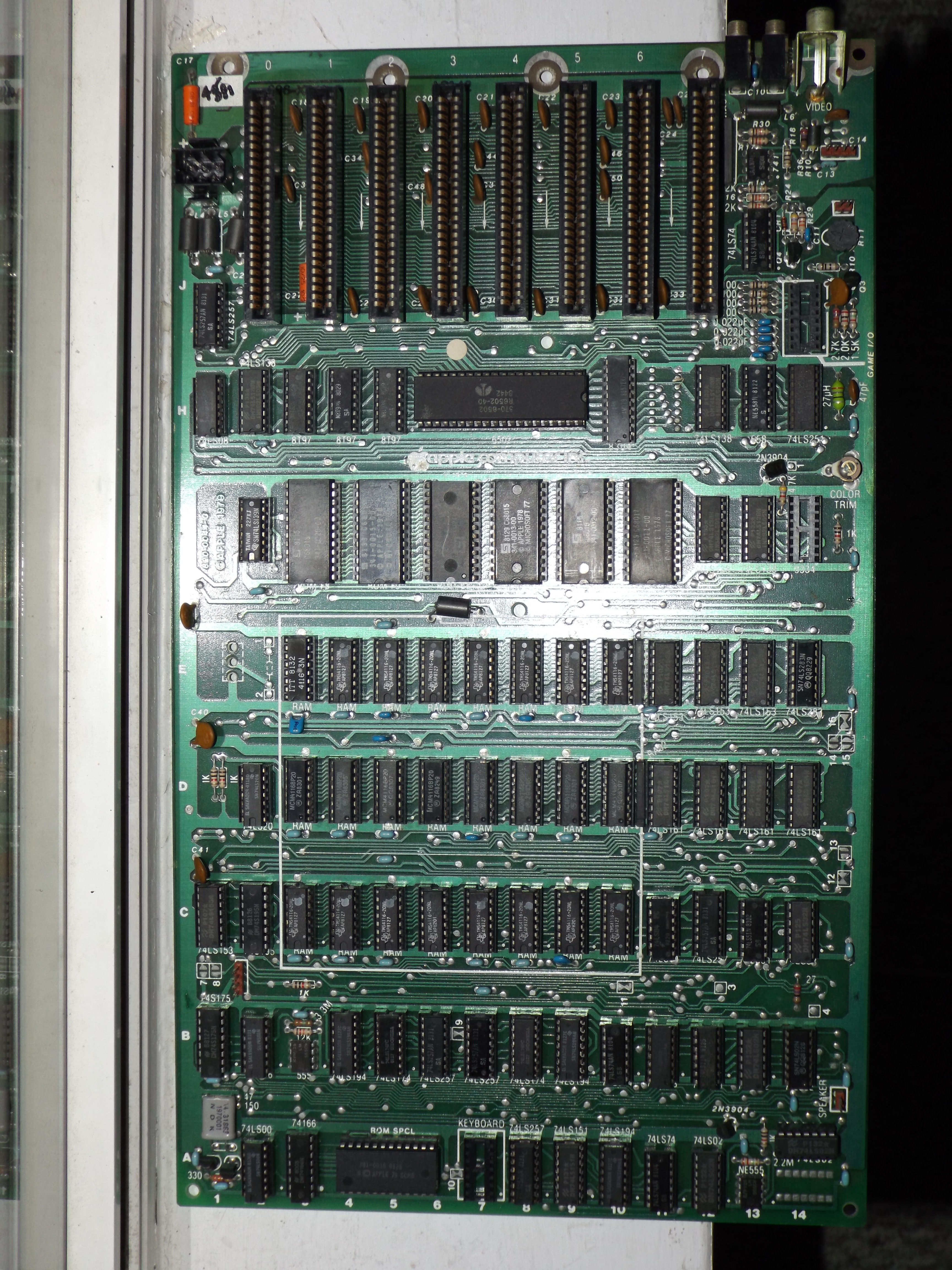
Here are high-res photos of the motherboard. As with my previous thread, I'll apologize for the poor lighting.
Whole board
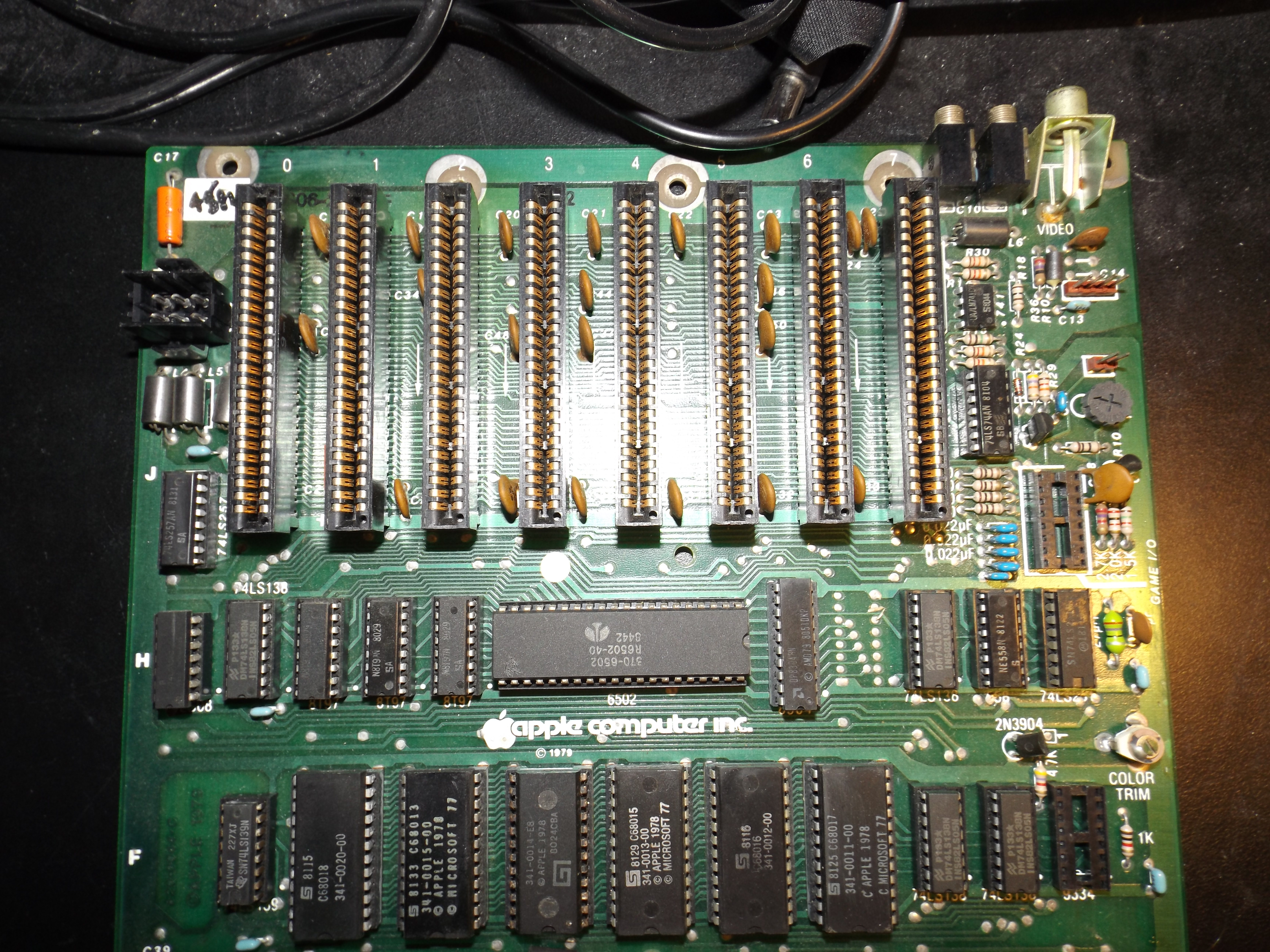
Closeup front third
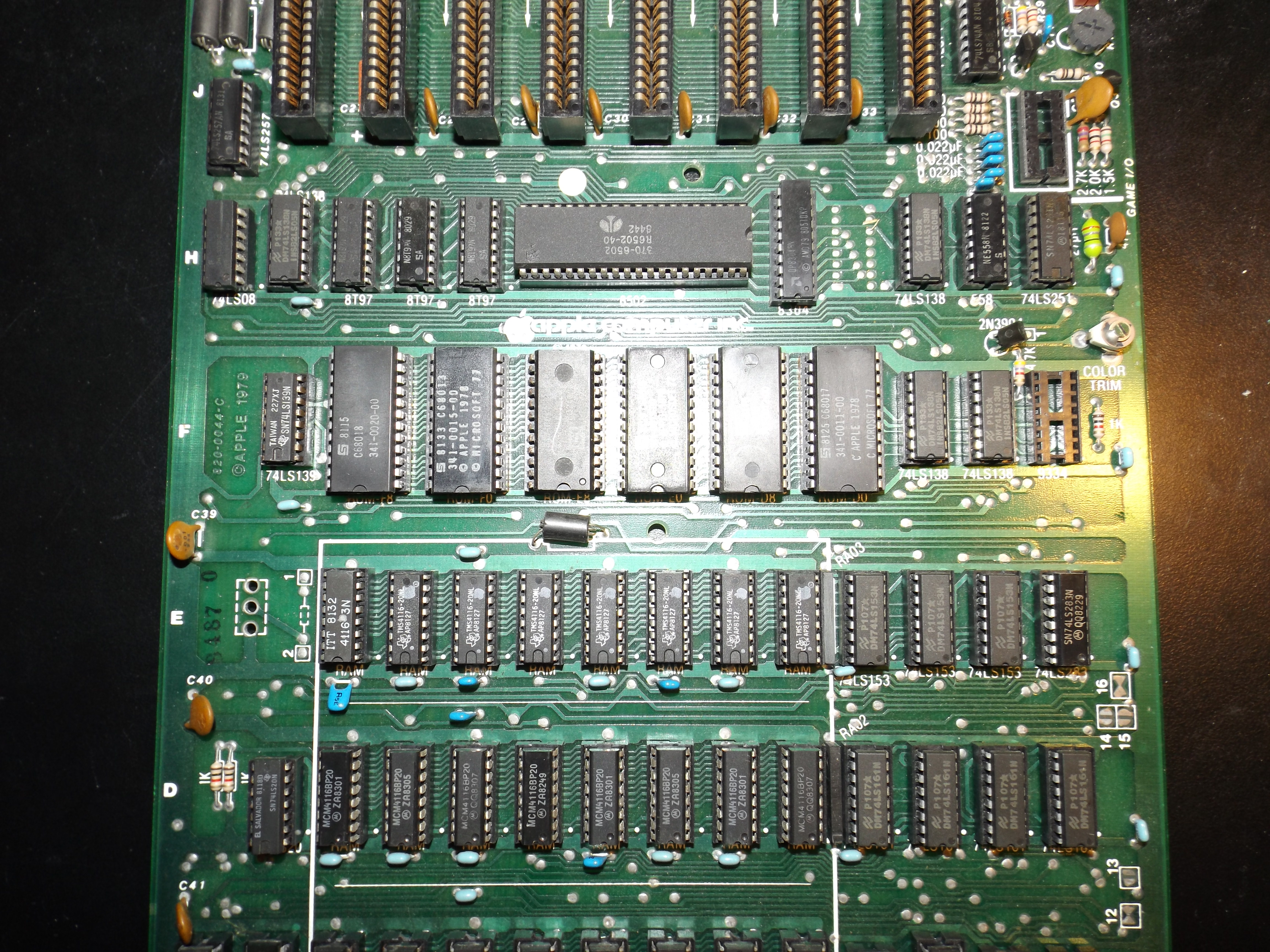
Closeup middle third
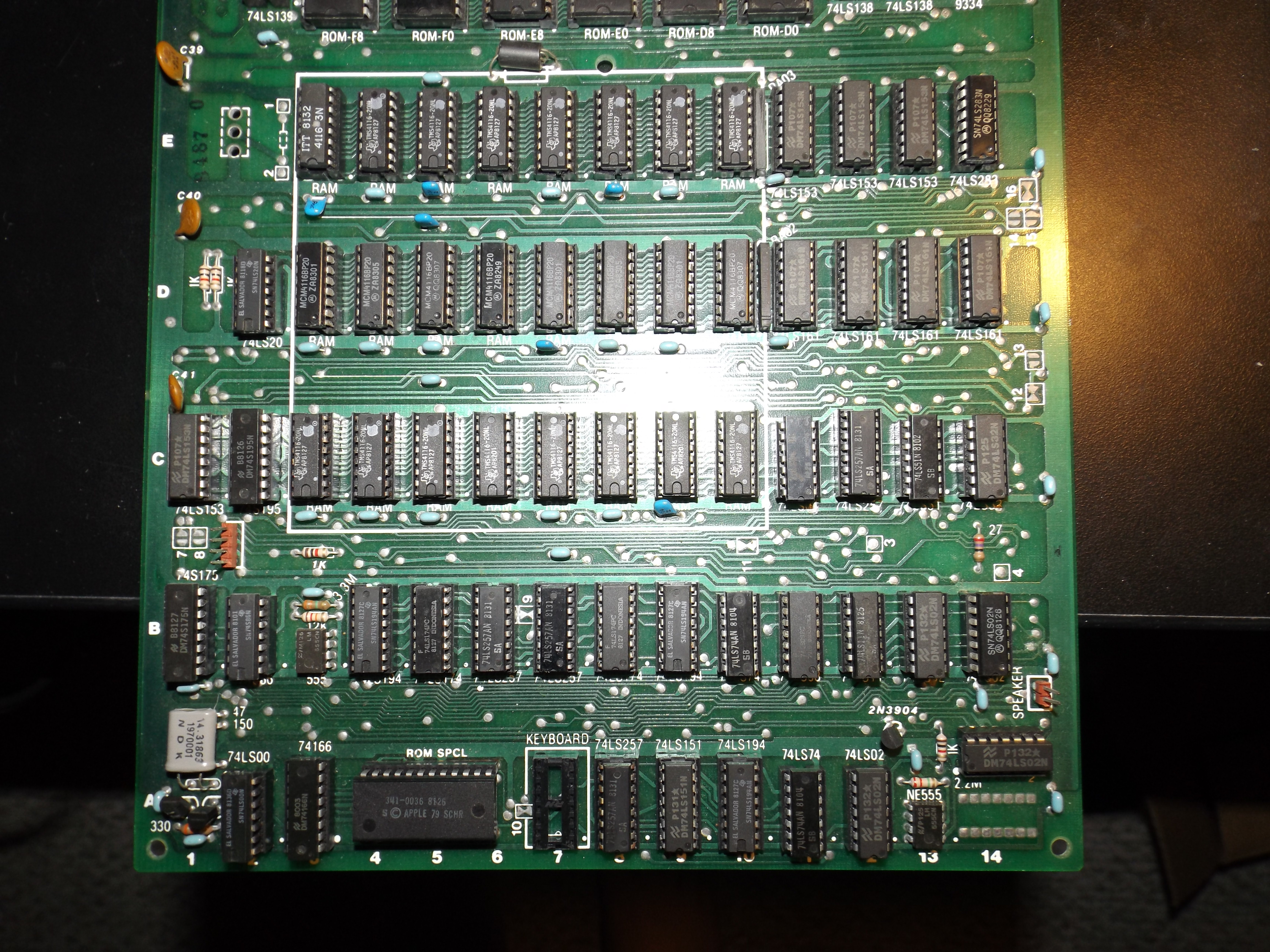
Closeup back third
Do note in the above photos that the E8 ROM is one of the bad chips I had tried on my other board. I installed it to fill the space, and to at least allow the system to boot into diagnostics once it reaches that level of functionality.
There is also a jumper wire on the bottom of the board. It is located behind the small "741" chip located at K13, connecting one of the pins to the resistor located immediately beneath it.
Jumper wire
And here are the date/revision markings on the board:
-Date code is 4881
-Revision code is 820-0044-C
-Near the revision code is the stamped code "8487 0"
-Behind the expansion slots are the two stamped codes "606-X548-F" and "A8142"
So, where should I begin?
Hello torindkflt,
same game like at last task....
i´ll work at the pictures and comment them....
with comments and description we´ll work along the task step by step...
if there are any questions don´t hesitate to post them....
I´ll post first extended reply tommorow...
sincerely speedyG
Hello torindkflt,
as mentioned by me in several previous threads the Apple II needs the following conditions fullfilled
to bootup to a prompt sign:
1. a mainboard with at least 16 kB of working RAM and and complete working chipset
2. a working powersupply
3. a keyboard plugged in
4. no interface card in any slot
so if the missing 9334 chip is not in the mailingbox the seller is proof of lie ! A mainboard without that
chip is NOT ABLE to boot up to prompt. The term "from working pull" indicates, that the mainboard
was extracted from a computer that boots up to prompt !
Back to the task.....
A and B: The chips marked "A" and "B" have been swapped in this board later - probably by repair...
they are not marked with "certification" stamp by apple ( that white tiny apple stamp at the chip ).
Swap out the entire set of chips at row C except of the one marked with the letter "C" and store
that chips on antistatic foam besides of the computer and put the ones marked "A" and "B" a bit
apart of the rest of the chips of that row !
D: Then swap out the entire set of chips from row D and place them also at the antistatic foam besides
of the computer !
E: swap out this chip to the antistatic foam ! This chip is marked by "3N" to be a very slow RAM chip
only certified to 300 nanoseconds while the rest of the RAM chips are marked to be certified to 200
nanoseconds ! This chip is predefinedd to be later relocated to a language card. Place it apart from the
rest of the chips at the antistatic foam !
F: relocate the entire rest of the chips in row E to row C ( except the extracted and separated chip marked "E"!
G: The two 74LS257 chips at location B6 and B7 handle the databus communication of the RAM ! Therefor it´s
recommended to make sure, that this 2 chips are as similar as possible ! Here they seem to be from different
fabrication line and date ( indicated by markings and shading of the case... ) while the chip at location C12
seems to match better with the chip at location B6 ! Therefor swap the 2 chips marked with "G" !
H: Of course the mainboard needs the 9334 chip at marked by "H" position. For testing that chip must be inserted !
next steps below the picture:
now after plugging the keyboard to the mainboard you may try to bootup the mainboard !
If the computer quits to a promt sign with "Apple ][" at the top of the screen and a ppropt sign with
blinking cursor at left side we will perform next step.
Otherwise if bootup fails - take new picture from screen and place here in next posting link to that new picture.
remark: It´s usefull while testing to have the speaker attached to the pins at location B15 !
some beep or not is another symtom to be mentioned in reporting post.
For better understanding it´s recommended to download this picture:
http://www.appleii-box.de/Bilder/Arbitrary.jpg
In this picture the function blocks of the computer are marked by different colors.
I might refer to this picture in later postings.
At the moment this picture might explain visually the swapping mentioned at "G".
sincerely
speedyG
I swapped the memory and LS257 chips as directed, then temporarily installed the 9334 from my working board. No luck, still shows garbage at power-on, but this time it's different.
Also, after running for about a minute or so (Just long enough for me to grab my camera), I began smelling a burning smell. I didn't see any smoke and I BRIEFLY felt around the board for any hot chips, but didn't find any. Still, something was definitely getting hot. Power supply is known to be good since it's the one I've been using in my working II Plus, unless there's a short of some type on the board that's damaging the power supply.
I hesitate to power it back on again, and I also hesitate to swap in any more chips from my working II Plus as I don't wish to damage those chips and end up killing that board again. But, if I absolutely must, I'm willing to try.
UPDATE: Found the hot chip, the 8T97 at H4. 30 seconds of power made it so hot that I could not touch it with the back of a finger. Temporarily replacing it with one from the working board didn't help though, still won't boot.
Hello torindkflt,
please also update in first posting links to new pictures taken from mainboard with new current status.....
is the keyboard now used the same that has been working with the repaired mainboard ?
waiting for the info....
add: please no further test unless next step is explained !
we don´t want to exceed any risks for working system !
it´s here in my place now 04:15 in the morning......
so i´ll in the meantime turn around for another bunch of sleep....
sincerely
speedyG
Ok, here's the board as it is right now:
After reducing memory to 16K
Again, apologies for the lighting. I thought setting the board in sunlight to take the picture would help, but obviously not.
I remembered I had a spare 8T97 left over from repairing the last board, so I stuck it in at H4 where the burning one used to be then did another power-on test to make sure that one wouldn't overheat, it didn't. I also, just for testing purposes, had swapped the other two 8T97s from the working board, but that didn't make any difference to the overall functionality. FYI, those other two 8T97s were apparently good, because the working board still works with them.
The keyboard is the one I've been using with the working board. I currently only have one case, keyboard and power supply, and I've been swapping it back and forth between the faulty and working boards as needed. I did consider purchasing an extra keyboard and power supply from eBay, but I couldn't find any that didn't also include a motherboard, which I'm currently not wanting.
I won't do anything else with the board until you say what needs to be done.
Hello torindkflt,
i´ll inspect the new picture and examine the circuitplans to post next steps....
the lighting of the previous pictures was poor but just well enough to enlighten it a bit with photoshop and get important parts visible... so up till now pictures are OK....
i´ll bear in mind your explenations about avoiding new purchase.... that´s OK too....
but for testing it is important to plug in the keyboard while performing the tests....
so it´s probably at the moment better too keep the keyboard removable status...
next steps will be posted tommorow morning ( i.e. 12 hours from now.... )
tests in the next 2 or 3 steps are limited just to swapping of some chips and checking if bootup behaviour changes....
in case such change occurs please also make a picture from changed monitor output....
I am able to trace some mistakes down to specific chips by viewing the pictures of monitor output....
the mistake at the 8T97 is not that surprizing....
there must have been previously an accident caused by an interface card and resulting to internal damage of that
adressing bus interface chip and the chip of course remained in damaged status even after the interfacecard has
been removed....
at the moment you may give a change/swap of the 2 74LS174 chips that are related to the databus a chance
by swapping them both with the chips in the working mainboard....
the 2 chips are located at B5 and B8. if behaviour while poweron changes the picture
please take picture and set link here.... otherwise you may leave the swapped chips in their locations - if the working mainboard also keeps after swapping in working status...
sincerely speedyG
Hello torindkflt,
Check at position marked by "!" in picture below.
If there is still that wire ! If yes - remove it immediatly !
( Danger of shortcut ! ')
Then test bootup if behaviour changes.
Next tasks:
questionmark: Is this one of the tested bad E8 or is it known to be good ?
If in doubt swap once with working mainboard .... and test working mainboard, if it´s still O.K.. ....
Check the 74LS166 at mainboard position A3 to be inseerted correct and firm in the socket.
A and B: First some cosmetic to remove dirt from socket spotted by arrow marked A.
Next swap 74LS08 in postion of each other marked B and perform next bootup text.
C: swap the 74LS257 with each other by position C and perform next bootup test.
D: swap the 74LS02 chips at positions marked D. Pay attention to orientation of the notches on the case and perform next bootup test!
E: swap the 74LS283 with the chip at the working mainboard and test both boards by bootup test and
check again for change in behaviour !
If at any stage of the tests the behaviour changes it indicates one of the swapped chips to be bad....
please take at that changed state again a picture from monitor output and leave here a link to that picture....
together with statement of last performed step in the tasklist.
You might then be able to detect the bad one by swapping with the working mainboard and test the working mainboard.
Bootup failing at the working mainboard indicates the swap of the bad chip and swapping back should put the
working mainboard back to working state. Then the bad chip must be marked to be replaced by new chip.
sincerely speedyG
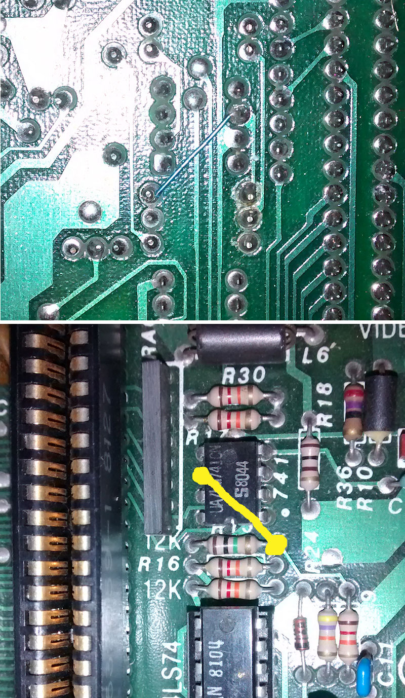
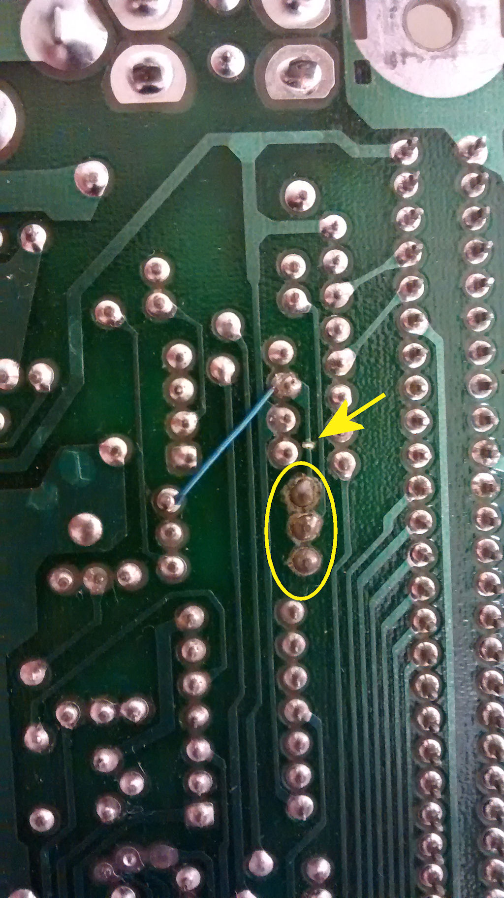
Ok...I could not find the extra wire you indicated should be removed, but while checking the back of the board again, look at what I found:
First, there's a cut trace that I presume is normal because of the green jumper wire. HOWEVER, the solder joints in the circled area appear to be bad! I assume this is at least part of the problem.
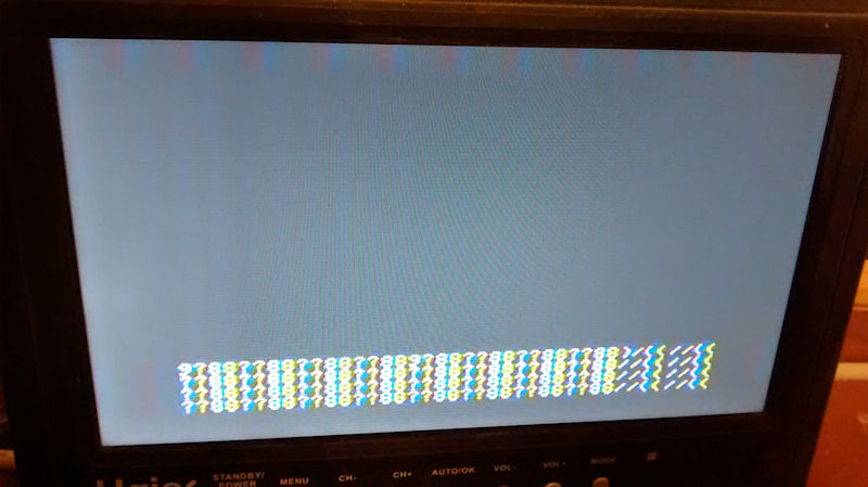
I did not observe any changes in the video output until I reached step D. After swapping the LS02 chips around, the display changed to the following:
I stopped at this point, I have not yet done step E. I wanted to wait for your input before proceeding.
Hello torindkflt,
so it seems next bad chip has been detected....
i´d make proposal to swap one by one the 2 chips with chips from the working board and then
check each chip by bootup of the working computer.
The one that causes the working computer to fail bootup is the bad one and must be replaced ....
then after both corrected chips are back again in the faulty mainbaord you should proceed with the
next step and testing....
it seems to get confirmed that at least with the current RAMbank there is no trouble...
if we get the faulty compter starting correct next stap later will be testing each row of the RAM-
chips now set besides to the antistatic foam row by row and testing - i will explain best procedure
when we get the flashing promt and correct bootup.
At the moment i still believe there is also another damaged chip on board ....
but we´ll find that "bad guy" too....
just proceed and mail new link to new picture when again new behavious rises upon horizon...
it seems the cut trace was mended by the added wire....
so far the videooutput is O.K. the mended area is related to the cassette port.
therefor it´s not that important at the moment...
i´d make proposal to keep that in mind and we might touch the mended area after the computer is up and running....
then we might turn back and check the cassette input and output... O.K. ?
But if you inspect carefully the solderside of the mainboard and find another damaged trace
make picture and leave here a link and a second larger view so that i´m abe to locate the area of damage...
in this case it was easy because it was for sure the solderside close to the 741 at the
cassetteport just besides of slot 7....
after your reply i´m now "off duty" heading for my pillow and some sleep...
i´ll check for your next replies tommorow morning while taking my tablets and sipping my breakfast coffee...
just an idea... if you inspect the solderside and take some pictures ( each maybe a 1/4 of the mainboard area...
maybe i find additional similar problems...
sincerely speedyG
It need be said that every now and then, the video does cut out while testing the board, and it won't even send a signal to the monitor. It's quite random though, and I have not yet found any possible link as to what might be causing that.
Ok, by using the working board for testing, I discovered that the Motorola LS02 is faulty, so I'll need to order it along with a replacement 9334. By the way, I read on another Apple II board that the 9334 can be replaced with a 74LS259. Is this correct?
Anyway, even after replacing both LS02 chips with known-good ones, there are no changes on the display. I find that odd since switching them around before caused a change.
I checked the bottom of the board again, and I did find another spot that could have bad solder, the back side of the RA02 resistor block.
RA02 Solder
This was the best picture I could get. Tomorrow when I can set it out in daylight, I'll take some more pictures of the entire bottom of the board.
Also, you asked earlier if the E8 ROM currently inserted is one of the bad ones. Yes it is, because I currently have only one known-good E8 ROM chip and don't want to damage it by repeatedly swapping it back and forth between the working and faulty boards. Once we get this board into a more functional state, I'll swap the working E8 ROM in. Ultimately I know I'll have to order another replacement E8, but considering the last four I bought all turned out to be bad, I must admit to being a bit discouraged about that prospect.
Hello torindkflt,
i´ll make at this point a summary ( and please accept, that it covers some topics in depth, bearing
in mind that this thread is also later revisited by newbies who might want to learn while making
attempts to repair their own mainboard too.... ):
When the Apple II is powered up and starts booting, it performs a kind of "To Do"-list ( i.e. code
from the ROMs )....:
it sets up a thing called "zeropage" in RAM in the lowest few hundred bytes
this zeropage contains some values collected while booting up - among that
values for example is the highest availiable RAM adress ( which it determines
by a very simple kind of memory testing, by peeking and pokeing some adresses
at top of 16kB, 32 kB, 48 kB and finally at 64kB.
If it recognizese 64 kB present then it starts loading a bunch of code to the languagecard -
If the testing for 64 kB fails it starts loading the code to normal memory below 48 kB,
depending to the amount of memory detected ( because after peeking and pokeing memory
it sets at the zeropage in one memorycell the adress representing "high-mem" and
while loading code from ROM and performing additional teating ( by scanning the slots for its contents )
it also raises the value stored in the memorycell representing "low-mem" meaning that memory
below of that adress is used by the systemcode loaded from ROM.
This happens before the Apple II even tries to access any diskdrive and tries to load operation system !
After completion of the "first stage of boot up" - the Apple II recognizes a diskcontroller to be
present in the system by scanning the slots from top ( slot 7 ) towards bottom ( slot 0 ).
This is also the reason why the Apple prefers every time to boot from highest slot.
If no diskcontroller or harddisk controller is present then the Apple II will quit to the
"promt" sign => "]" at the left top side, one line below of the "APPLE ]["-title centered in the topline
and a blinking square, marking the cursor position behind the prompt.
Due to the fact that no bootable device controller was detected it then will wait for commands to be
entered either as basic program or to recieve instruction for loading code from the cassette input.
At this state the zeropage contains allready all values related to the system and collected during the
"first boot stage" - also indicating some basic adessses like "reset-vector" several adresses
related to routines in ROM ( like starting adress for load routines ) and dependent to the ROM´s
present in the system ( Integer or Applesoft, language card present or not, Autostart ROM or not ).
If any crash occurs in this "first boot stage" the system will "freeze" in variable kind of displays
depending to the adress the system crashed at.....
If system crashes while loading operation system from Disk or Tape it will more likely crash
to machine code level used by the so called "Monitor" and this is not meaning the display
but instead a kind of assemblercode level program and this is indicated by a
"*" prompt followed by a set of machine code bytes dumped to the screen.
Back to the "first stage crash":
Depending to the display at screen an experienced user might be able to assume a range of adresses
within the crash might have occured - indicated by crashing at level of Textpage area, Mixed mode
display area ( thats the kind of screen with 4 lines of text at the bottom and pixel display in the
rest of the graphics page display ) or if the crash occurs in the area allocated to one of the
graphic pages ....
In very early parts of crashing the display will only display solid square light areas or blinking
graphic symbols ( this indicates that the system is not even able to access the character ROM
correct - and it often indicates damaged RAM or severe mistake or shortcut at the datalines D0 to D7.
At this system analyzed in present situation the first crashes occured in early state displaying the
normal characters - so it was simple to resume that at least the datalines must be O.K. and the trouble
must be allocated within the adressing lines of the system.
Second crash-picture displays so called "mixed mode" ( explained above as mixing of text and graphics )
- so this happened in a later stage than the previous crash-screen....
So from this point the analysis must asume the lower adressing range from A0 to A7 or A8 to be O.K.
and the trouble must be allocated in the area from A8 or A9 to A15.
Or it might indicate a RAM chip to be only partially working correct at low adresses but having trouble
with adressing higher adressing ranges in the chip.
So that´s the "state of art" at the moment in this buggy system.
now back to this thread itself and to you torindkflt,
as mentioned in previous posting the wire modification at the 741 is related to the cassette port.
Here is more detailed explenation:
The 741 is an operational amplifier that amplifies a signal coming from the cassette port to the system
as serial "read in port". In general the amplification of the signal is determined by a so called
"feedback resistor". That´s in the following picture the 1 M resistor ( one Mega Ohm ).
In this system somebody has cut one trace and "by-passed" by wire that "feedback resistor" with the
result, that the signal is also sent back to the non-inverting input pin of the OPamp
straight ahead - this causes the 741 not to perform amplification but instead just only inverting the signal !
There is a wide spread of different 741 chips out there with different amplfication parameters....
This one seems to have allready a quite high internal amplification without any need of correction
by the "feedback-resistor" .... and therfor it was bridged by the user or service-technician.
Maybe one of the possible reasons was, that the used cassette recorder had very high output level
and the user was not able to regulate output of that tape-unit that far lower requested by the Apple
and therefor the input branch of the computer was limited by this modification to acceppt that
high input level without any amplification - just inverting the signal and cleaning the dirt of the signal.
Anyhow:
This is only relevant if you intend to load software from cassette recorder and has no effect to the
other functions of the computer.... that´s the reason i made proposal, not to care about that
modification at the moment....
If you intend to use a cassette recorder later for storage then it might become later important
to remove the modification depending to the kind of taperecorder you intend to use....
But now to the current task:
Your last question: YES - the 9334 chip may be replaced by a 74LS259 !
Even in the most circuitplans there is a 74LS259 displayed at that position.
That chip is responsible for switching the display modes between text, mixed and graphic pages.
have a look at the part of the circuitplan below and the circled chip:
Now some remarks to the testing of this mainboard:
In fact the working E8 ROM was taken from this mainboard for repair of the other mainboard.
But the E8 ROM was damaged by the other mainboard - which is now in working state !
This mainboard did not damage the E8 ROM and i don´t believe there is any danger
by using that working E8 ROM in this board !
The damage in this mainboard was caused by inserting a damaged interface card that killed the 8T97 chip at location H4
and one or two other chips at the board.
Without use of that damaged killing interface card i can´t believe the E8 ROM being at risk of getting damaged !
THEREFOR IT IS UPMOST IMPORTANT TO USE THE WORKING E8 ROM ÍN THIS MAINBOARD WHILE TESTING !
But of course while moving the E8 ROM you must carry our the duties of care -
carefully lifting the chip while extraction and -
carefull insertion in the socket -
of course with upmost care to the pins ( no bending or breaking force )
and of course correct insertion ( with notch on the chip in correct position ) orientation !
So each time a move is performed - it´s highly recommended to "double check" this points
before performing a short powerup for testing !
About the RA02:
Check of the trace marked by 1 if it is damaged /cut/disrupted by multimeter and continuity !
And 2 checkout this marked points not to make shortcut with siding trace or siding soldering point !
Use magifying glass and check by mutimeter - remember : This measurements are performed at
network of resistors - so values of 1 kiloOhm might be correct !
But values below 500 Ohms are for sure bad !
So use for measurement the range closest above 1 kilo-ohm ( at most multimeters that will be the range of 2K ).
then perform remaining tests with working 74LS02 ( alternate taken from working mainboard )
with same precautions as explained to the E8 ROM and report results here.
sincerely
speedyG
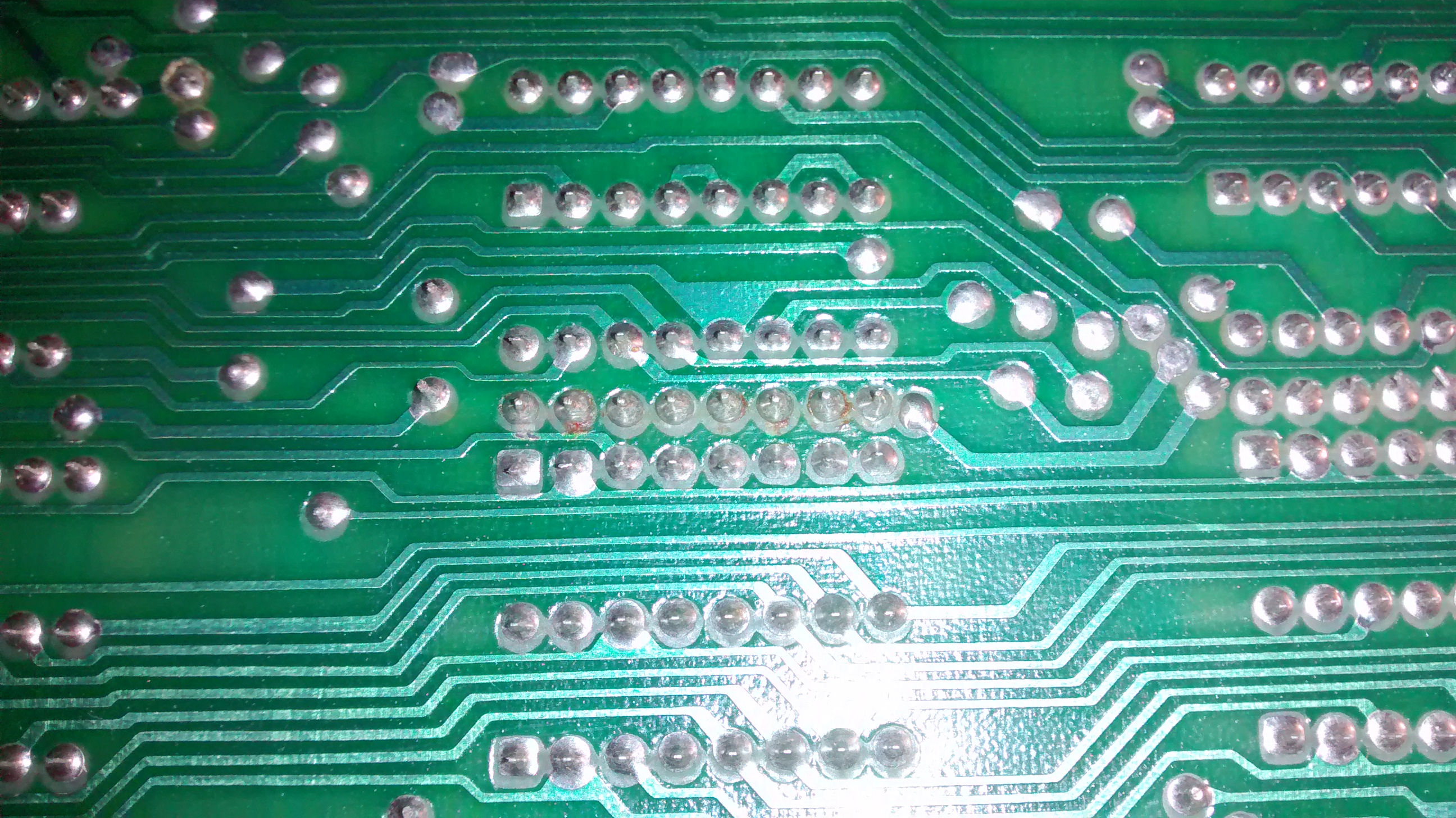
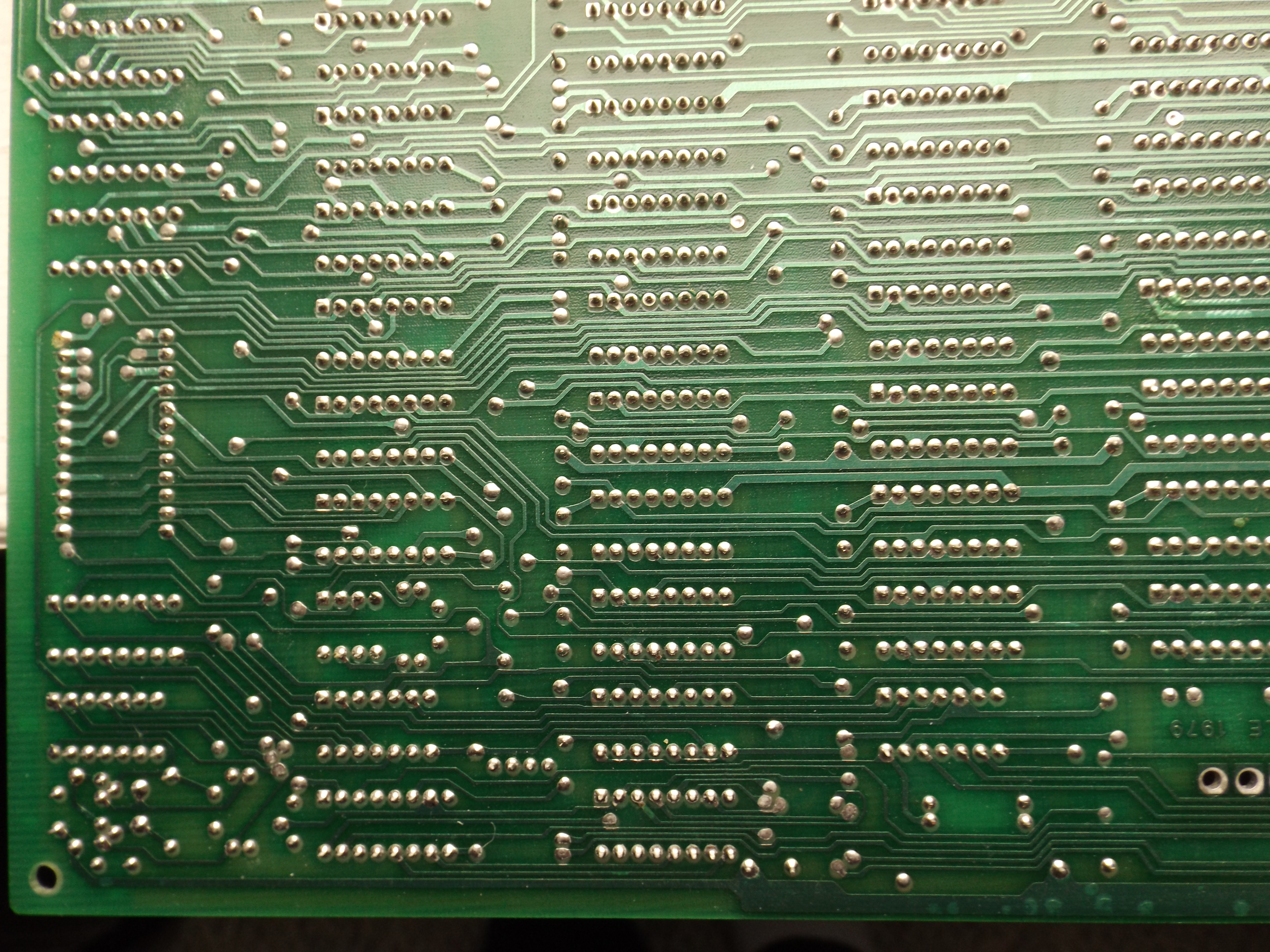
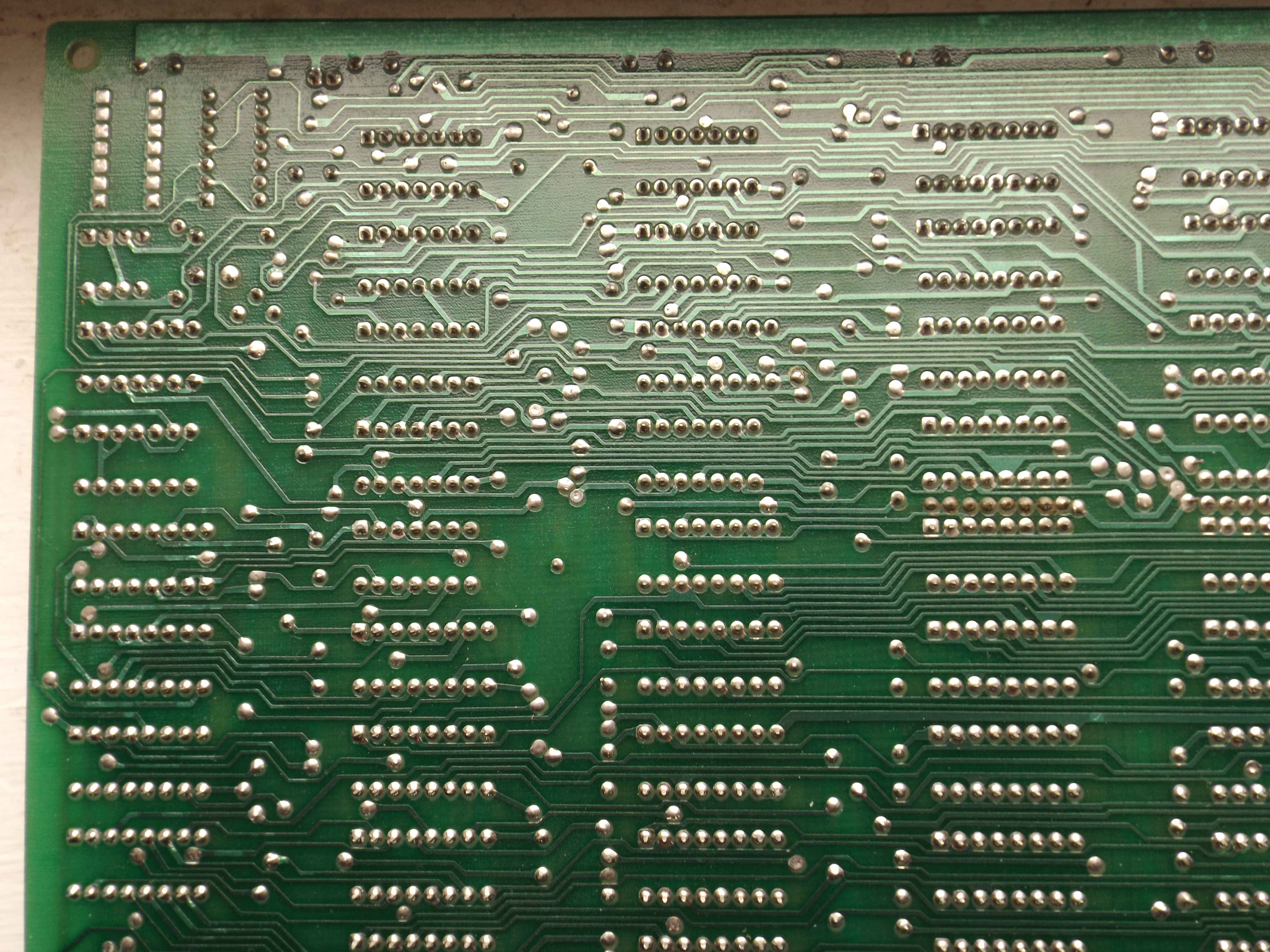
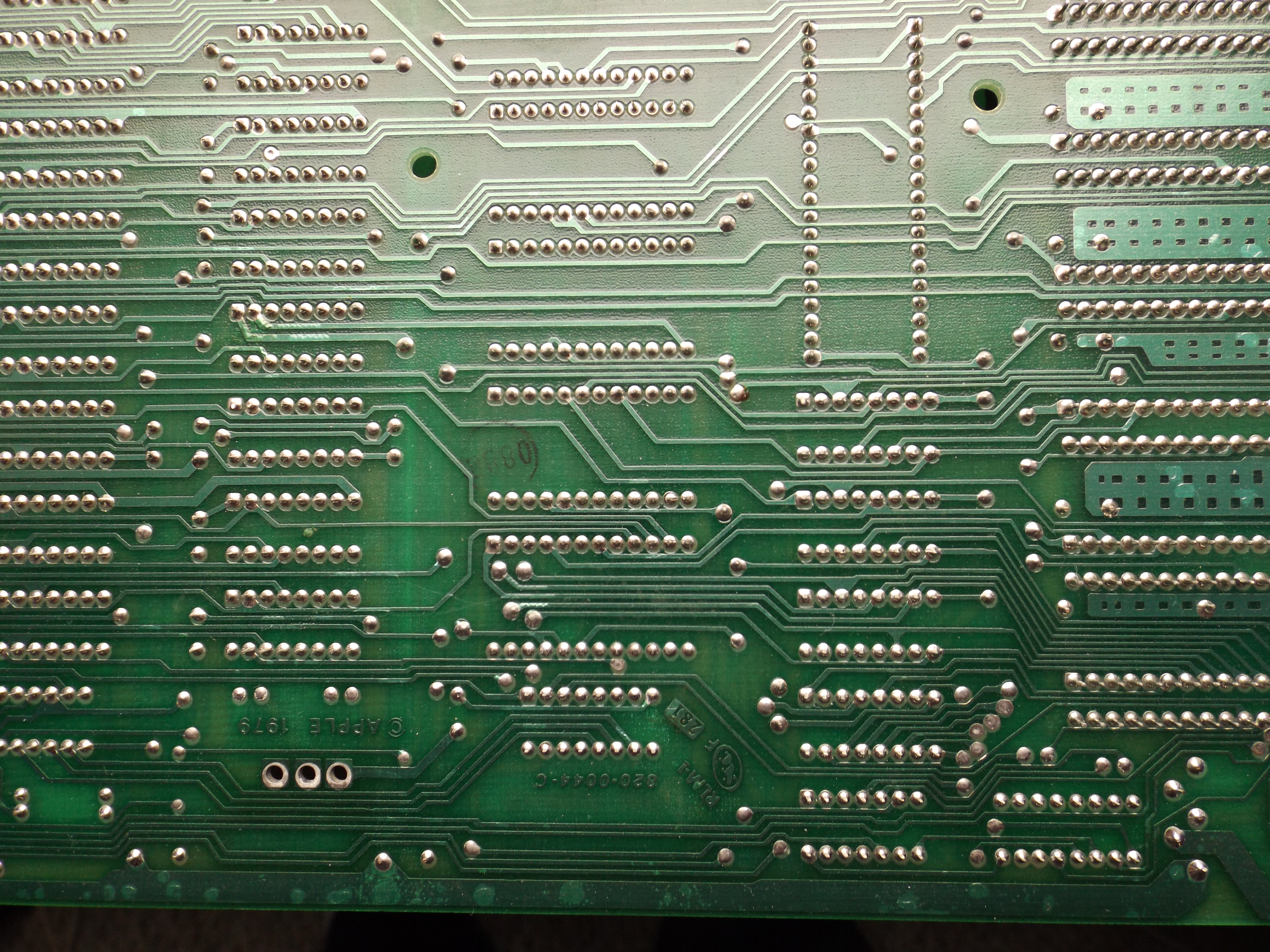
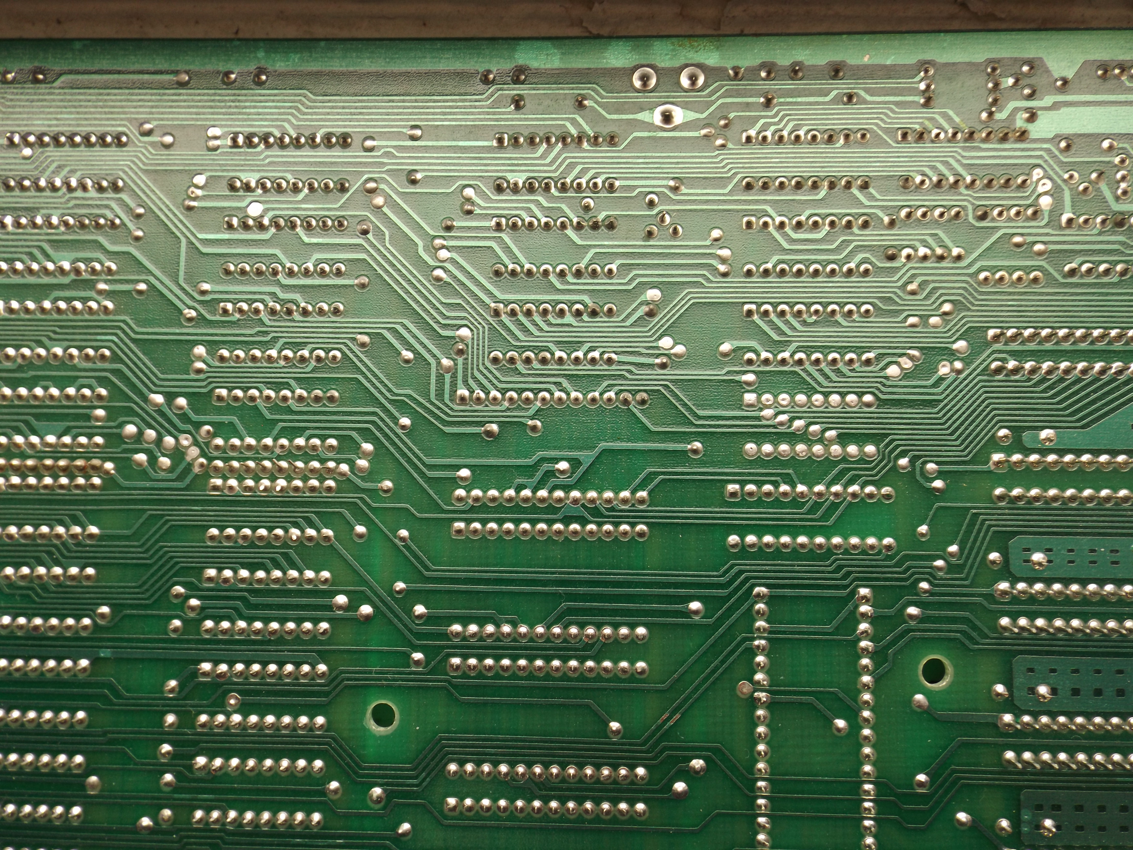
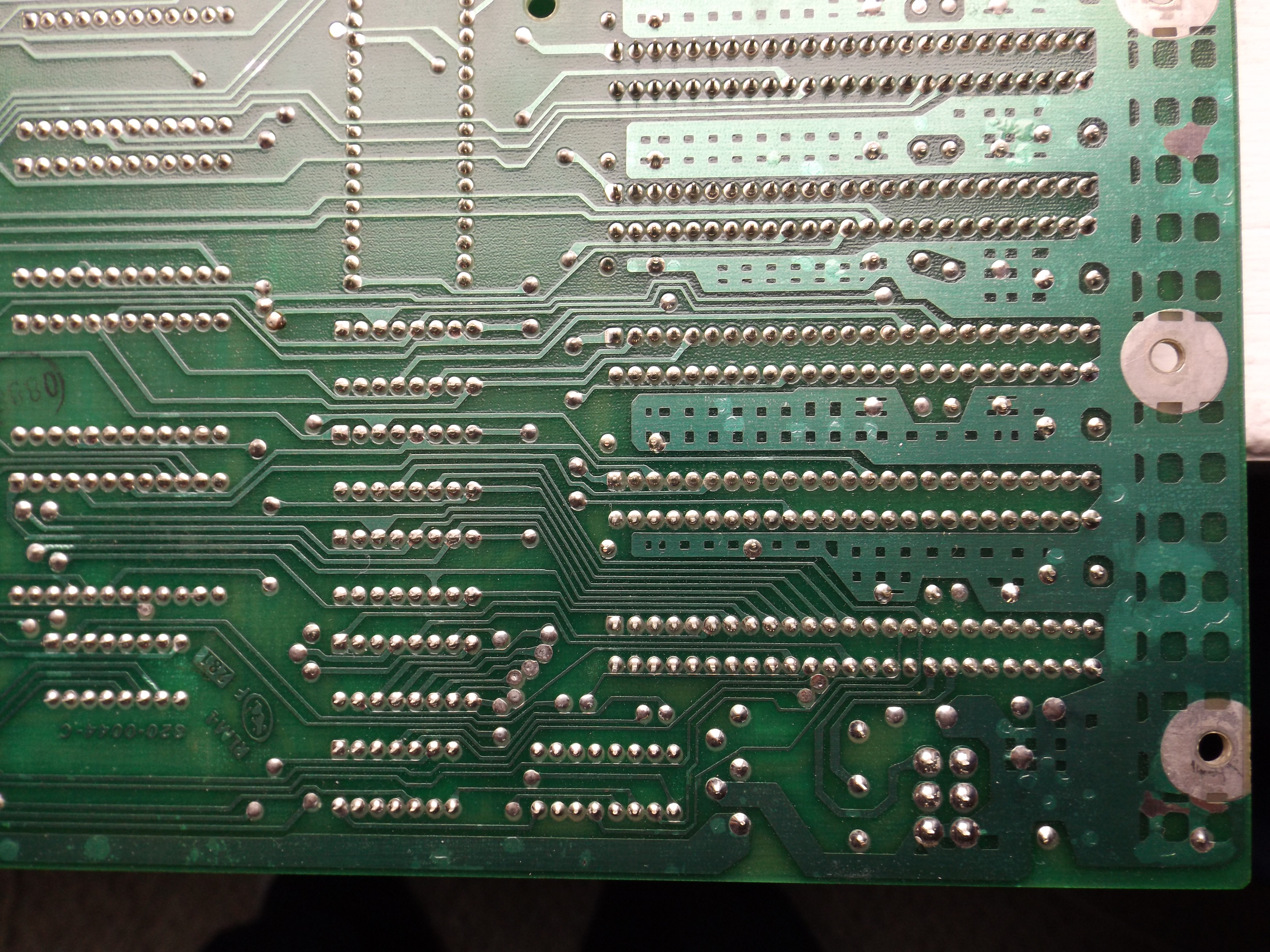
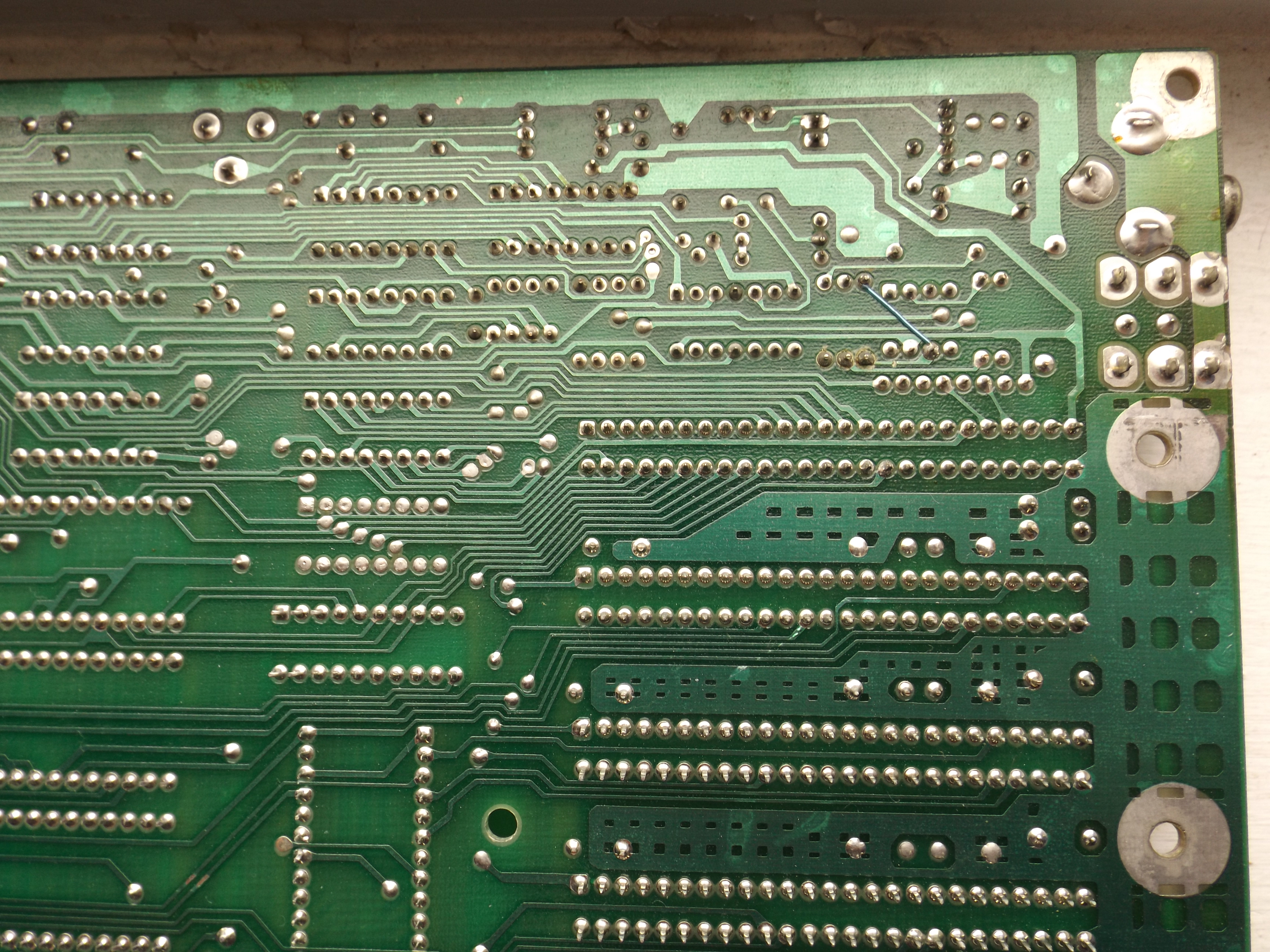
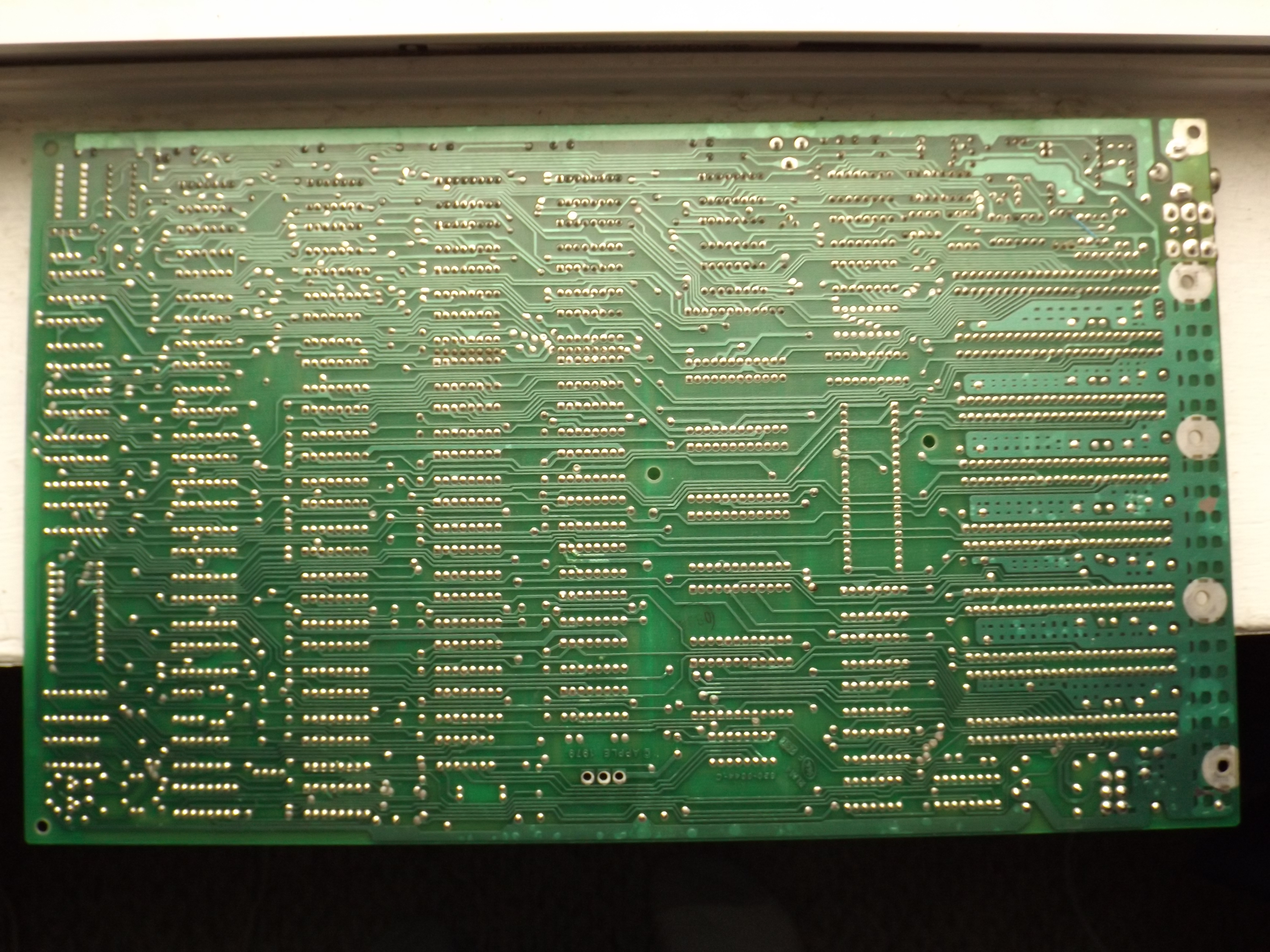
I do not currently have time to do any further testing on the board as my lunch break is too short, so that will have to wait until tonight. However, I did take some high-res pictures of the bottom side of the board for your review. These were taken with the slots on the right side of the board:
Whole Board
Upper Left
Lower Left
Upper Middle
Lower Middle
Upper Right
Lower Right
I'll work more on the board when I have time later.
Hello torindkflt,
in the meantime i have taken a view to the pictures...
due to the fact that they have quite large size i also only place here a link to the marked pictures.
Also due to the limited size of my site i will have to remove them in few days ...
so plaese download them for later use.
In general i just have marked by arrows the suspected soldering joints that you should inspect,
probably clean and resolder them....
At the resistor networks the remaining pinwires are to long and should be shortened down
by use of a wirecutter to avoid possible bending and shortcuts...
http://www.appleii-box.de/Bilder/W1Alow.jpg
http://www.appleii-box.de/Bilder/W1Ahigh.jpg
http://www.appleii-box.de/Bilder/W1Dlow.jpg
http://www.appleii-box.de/Bilder/W1Dhigh.jpg
http://www.appleii-box.de/Bilder/W1Hlow.jpg
http://www.appleii-box.de/Bilder/W1Hhigh.jpg
The 2 traces marked by "A" should be cleaned and after cleaning covered by small portion of
gloss paint to protect the trace from oxydation/coroding.
sincerely
speedyG
Apologies for the delay, I've been busy preparing for the holidays.
I currently do not have a soldering iron, so redoing any of the solder joints is not possible at this time. I did inspect them with visually and with a multimeter however, and I couldn't find anything outwardly suspicious aside from a bit of oxidation and dust. As for the exposed traces, I'll have to see if I can find some paint to cover them over with.
What is the significance of the point marked "B" in the image W1Dhigh? You neglected to mention that in your previous message. Also, what should my next step be?
Hello torindkflt,
don´t mind about delay.... nearly all folks are now busy for holidays ahead........
B mentions the wires to be to long and bearing danger of short circuit..... the extended wires above the
soldering joints at the resistor network should be cut off.....
The problem with oxydated soldering joints is a bit more serious....
such joints get worse contact by rising resistance.....
next step missing was:
E: swap the 74LS283 with the chip at the working mainboard and test both boards by bootup test and
check again for change in behaviour !
If at any stage of the tests the behaviour changes it indicates one of the swapped chips to be bad....
please take at that changed state again a picture from monitor output and leave here a link to that picture....
together with statement of last performed step in the tasklist.
You might then be able to detect the bad one by swapping with the working mainboard and test the working mainboard.
Bootup failing at the working mainboard indicates the swap of the bad chip and swapping back should put the
working mainboard back to working state. Then the bad chip must be marked to be replaced by new chip.
bearing in mind the explenation of:
Your last question: YES - the 9334 chip may be replaced by a 74LS259 !
Even in the most circuitplans there is a 74LS259 displayed at that position.
That chip is responsible for switching the display modes between text, mixed and graphic pages.
and for testing at least one kind of working chip must be in that socket !
Now some remarks to the testing of this mainboard:
In fact the working E8 ROM was taken from this mainboard for repair of the other mainboard.
But the E8 ROM was damaged by the other mainboard - which is now in working state !
This mainboard did not damage the E8 ROM and i don´t believe there is any danger
by using that working E8 ROM in this board !
The damage in this mainboard was caused by inserting a damaged interface card that killed the 8T97 chip at location H4
and one or two other chips at the board.
Without use of that damaged killing interface card i can´t believe the E8 ROM being at risk of getting damaged !
THEREFOR IT IS UPMOST IMPORTANT TO USE THE WORKING E8 ROM ÍN THIS MAINBOARD WHILE TESTING !
But of course while moving the E8 ROM you must carry our the duties of care -
carefully lifting the chip while extraction and -
carefull insertion in the socket -
of course with upmost care to the pins ( no bending or breaking force )
and of course correct insertion ( with notch on the chip in correct position ) orientation !
So each time a move is performed - it´s highly recommended to "double check" this points
before performing a short powerup for testing !
About the RA02:
Check of the trace marked by 1 if it is damaged /cut/disrupted by multimeter and continuity !
And 2 checkout this marked points not to make shortcut with siding trace or siding soldering point !
Use magifying glass and check by mutimeter - remember : This measurements are performed at
network of resistors - so values of 1 kiloOhm might be correct !
But values below 500 Ohms are for sure bad !
So use for measurement the range closest above 1 kilo-ohm ( at most multimeters that will be the range of 2K ).
F:
and next tests would be swapping out chip by chip RAMchips from the mainboard
with RAMchips removed formerly from ROW C and set aside at antistatic foam
before swapping in Chips from Row E
( still keeping a row of "certified" chips with the "white apple logo on chip"
(still only with one row of RAM chips i.e. 16 kB while performing tests ) and
checking after each single chip swapped the bootup behaviour of the computer
and thereby checking each RAMchip for function ( change in behaviour will indicate a faulty RAM chip ).
( and of course all test with working 74LS02 bearing in mind
that the damaged chip most be sorted apart while testing )
sincerely
speedyG