Hi,I'm looking for any informations, schematics, component references about the Lisa 1 motherboard.
For my card, the references are 620-0108-E & 820-4013-C but any informations with other revisions are welcome.
Lot of components are completely destroyed and some PCB traces are cut.
I need to find and remplace them, but I have no reference/value…
Is there a schematic? I haven't found it.
Thanks to help me to restore this computer.
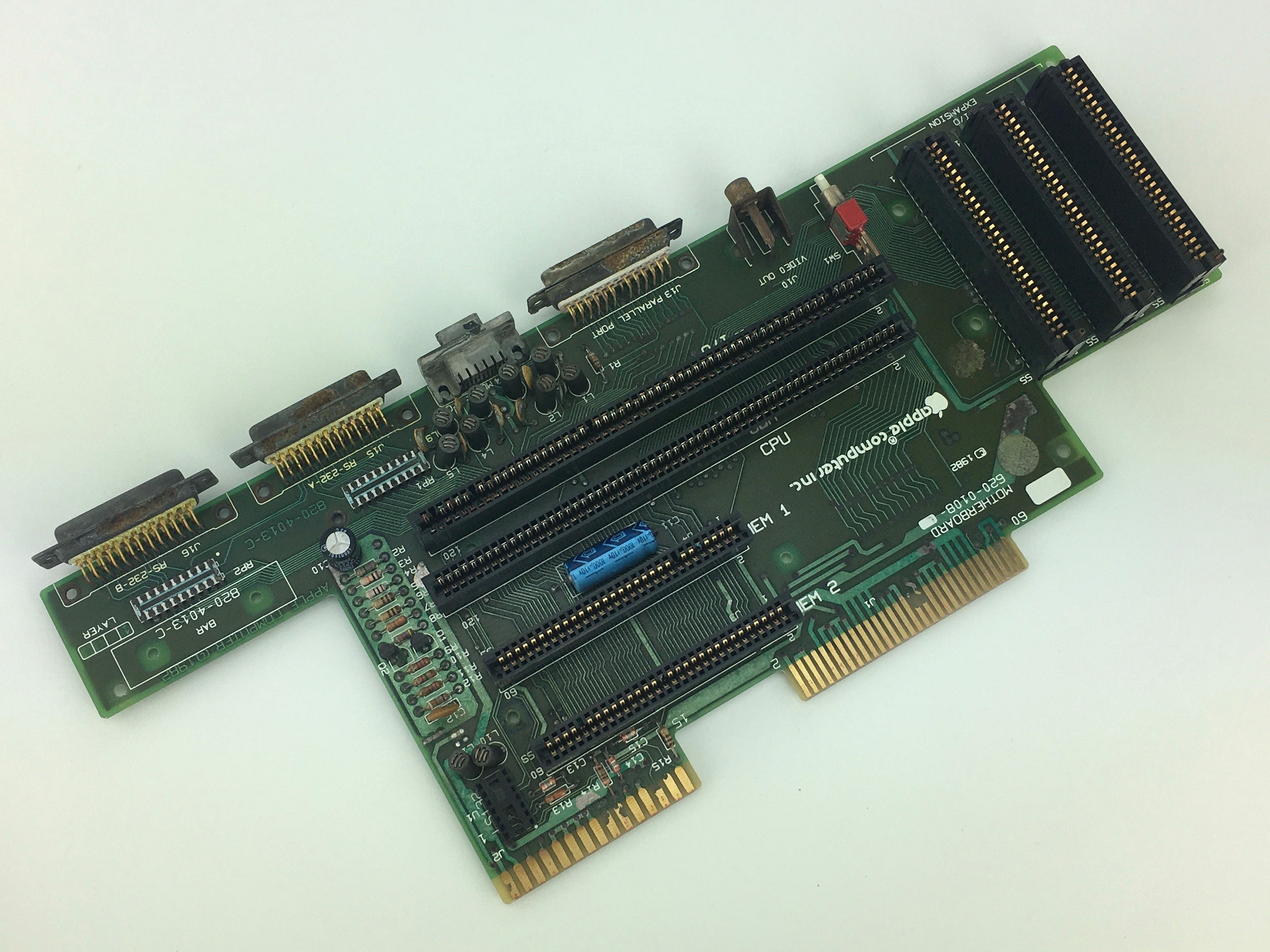
Looks like your motherboard might be beyond repair. The gold edge connectors and card-edge connectors are not looking very good.
I have a motherboard in much better shape, actually an entire cage assembly, but when I look at the Memory Board card-edge connectors, I see a bit of "frost" on the surface of them.
If I were doing a restoration, I would likely replace them. Being such a large connector with so many pins, it takes expertise to extract the connector without harming the motherboard.
Fortunately, I have the equipment and expertise to do so. If this is something you are interested in, let me know. Those connectors are still available.
I also have a spare Microprocessor board in good physical condition, a spare I/O board in fair physical condition, (some bubbling at the edge connector) and 2 512K memory boards in excellent condition.
None of these, including the motherboard, have been tested, as I no longer have a Lisa available. I am in the USA, so shipping is also something you might want to consider.
Let me know if this is something you are interested in.
Lisa Motherboard.jpg
Mem Connectors.jpg
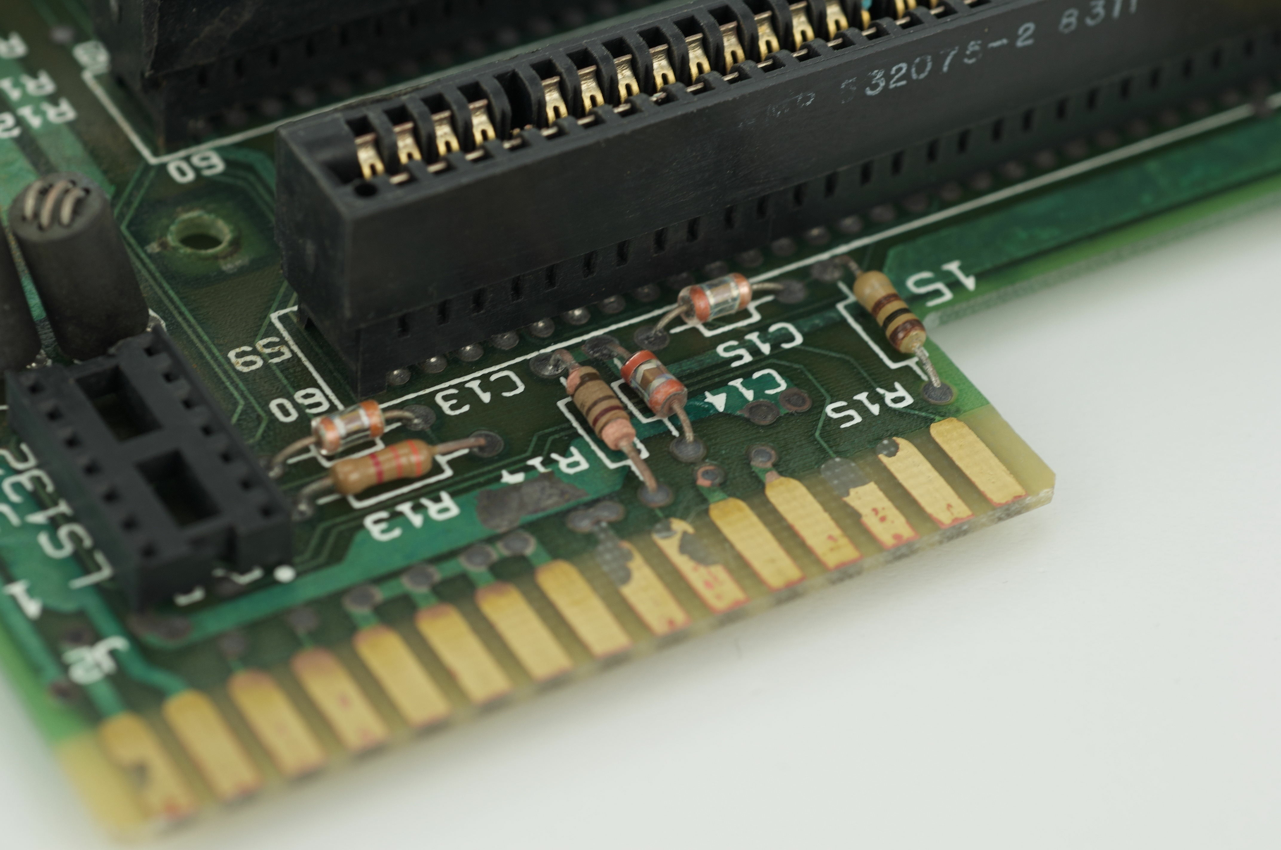
Thanks for your interest.For now, I'd try to restore it, as the other cards (CPU, I/O, RAM…).In fact, I've removed the connectors since the previous pictures.The next picture is not updated too, since I've removed capacitors and choke inductors near mouse port.I've found the four missing connectors, the reset buton, and the other external connectors.That's why I'm looking for values/references and motherboard schematic.
IMG_4779v2.jpg
I admire your efforts. Given the damage to the board, I'm not sure I personally would take on this level of repair. Definately a challenge.
I was recently trying to unsolder components on a corroded I/O board and had difficulty melting the solder. The oxydation on the joints made it very difficult.
I expect you will have trouble repairing the via's. You might end up etching to remove them and re-pinning them. (a lot of work given the quantity on the board)
I wish you success with your project.
As far as I recall, other than a revision ID, there is nothing that differs on the PCB logic between Lisa 1 and Lisa 2. Years ago, our Lisa systems were Lisa '1', and we 'upgraded' them to Lisa 2/5 systems, which only involved a ROM change and the 400K SONY drive swapout, plus the front bezel.
How are the Lisa-2 schematics inaccurate for this repair?
https://lisa.sunder.net/cgi-bin/bookview2.cgi?zoom=0?image=0?book=6
Tip here: Before you de-solder, use a normal (not high acidity) flux pen, and stripe it across all joints. Then, use a normal tinned iron to melt each joint (80W wedge tip works best), until they flow nicely.
After that, you can desolder far more cleanly.
Re: Tip: Before you de-solder, use a normal (not high acidity) flux pen, and stripe it across all joints.
Then, use a normal tinned iron to melt each joint (80W wedge tip works best), until they flow nicely.
A little easier said than done in this case ... I found that highly oxydized solder joints tend to crumble, not melt.
I tried "drowning" the joint in flux, (plumbers paste works well for this) but no matter how hard I try,
-even attempting to feed fresh 60/40 into the joint, the solder would not flow. It would only crumble.
In most cases, the via crumbled with it. These are severe in nature and difficult to repair.
How long have you let the flux sit in place? I suppose you could use an active flux paste in the worst cases. What iron wattage and tip style are you using, and what temperature?
There are times that you do want high-temp to force joints to snap back. The elasticity of the original solder should be recoverable, though. I've worked on solder joints from the early 70s recently and I've seen some rather heavily oxidised stuff, but I haven't had it crumble apart.
If you have any completely toast/generally worthless board with joints in that state, I would not mind examining it to see if I can get them to flow, and what it takes for me to accomplish it.
I was actually thinking about sending you my I/O board so you can see first-hand what I mean.
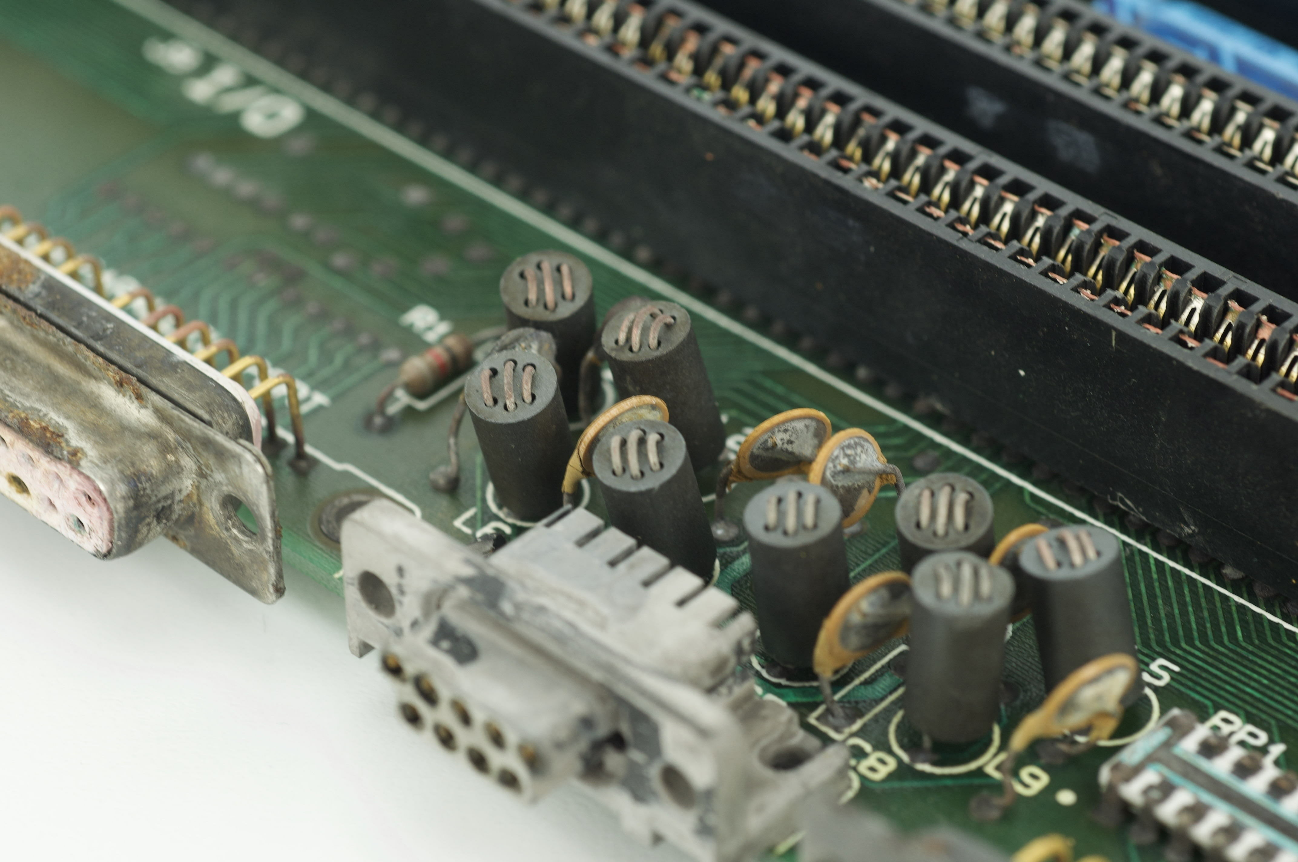
The oxydation around the 3-legged switch (near the battery) is oxydized so bad that the solder around it is totally black.
I was able to remove the battery leads from the board, (battery removed a couple decades ago) but in doing do, I noticed the solder 'flake" away from the hole as if it was totally oxydized and no longer flow-able metal. Much of it came through as a powdery mix, as if the lead compound had completely oxydized.
I use a variable temp Weller soldering station which I adjust between 400 and 600 Deg F, depending on what I'm doing.
I've tried through those temp ranges, but I don't like trying at 600 F because you can lift / burn pads pretty easy at that temp if you're not really careful.
My next thought was to grind the lead nearly flat (on the solder side) using a dremel and see if there is any metalic property left within the solder itself. As it sits, the solder joint is totally black.
Without flow, all I can do at that point is to etch the hole and re-pin the VIA. At least that's how it looks right now. I can post a close-up photo if you think it's of value.
Addendum: I have an array of Weller Soldering stations at my workdesk ranging from a very fine point tip to a wedge blade to 3/16 screwdriver tip. (and others)
I also use a Pace Desoldering station and a Weller hot air flow station for SMD work where appropriate. I've been soldering professionally for several decades and consider myself quite skilled at it, but I won't ever say say I can't learn something new -especially in the field of restoration, as most of my work was / is with up-building rather than restoration.
I would certainly be interested in seeing it, or working on it. In what conditions did it sit to extrude pure Pb12O19 like that? I have seen some dark and dull joints on boards as old as '71, but from '83?! That is uncanny.
Crystal formation of that sort in that time interval would in theory require an exceptional oxidising agent. If it is indeed forming like that, it is probably separating the pads and vias due to crystal growth; rather than due to heat or reworking. i.e., the damage was already there, but not visible.
I don't think I have seen this on 60s transistor radios or anything else that I've restored. Is this common especially on Lisa stuff for some odd reason, or was it unique to that one system?
Hi,
Thank you for your answers and encouragement.Actually, I was expecting to find a schematic just for this motherboard, not for the entire Lisa.I knew about the https://lisaem.sunder.net link, and I'd already downloaded the schematics.I'm going to try my best to save that motherboard. I don't know if the time/money spent will be profitable and especially if this Lisa will work again with all its original cards, the others being obviously less affected, but also damaged by the corrosion of the batteries.
Best regards,Patrice Freney
When you say 'profitable', is the goal of this project to sell the system when you are done?
Do you still have any of the Lisa Boards available, macnoyd? My Lisa 1's main logic board is toast and I need a replacement. Would you be open to selling them to me?
See your PM and post a photo to me. I can do the same.
I 'm working on this motherboard. I'm almost done with it excecpt for a few parts.
Can someone verify the value of the caps connected on the 9 pin connector inductors.
There is an old handdrawn image that shows the value as .01 uf.
However testing the two originals that didn't crumble to dust shows .001 uf.
TIA
ps: Since there isn't much data ont this board I'm attaching a netlist and partial schematic I worked out.
circuit.png
Uploaded wrong files
circuit.png
By searching online for "LC low-pass filter calculator", you can calculate the cutoff frequency given L=10 µH and C=0.01 or 0.001 µF.
The difference in cutoff frequency isn't great; around 0.5 MHz for 10 nF, or 1.0 MHz for 1 nF.
Th maximum pulse rate from the mouse is something like 400 dpi * (5 inches / 0.1 sec), or 20 kHz, so half a MHz bandwidth is more than adequate. The only reason I can see for changing to a higher filter frequency is to increase the dV/dt slope of the pulse edges.
Hi, maybe here you could find some more interesting info: https://github.com/alexthecat123/Lisa-PCBs