
| Attachment | Size |
|---|---|
| 1.92 MB | |
| 1.7 MB | |
| 23.43 KB |
Hi Everyone,
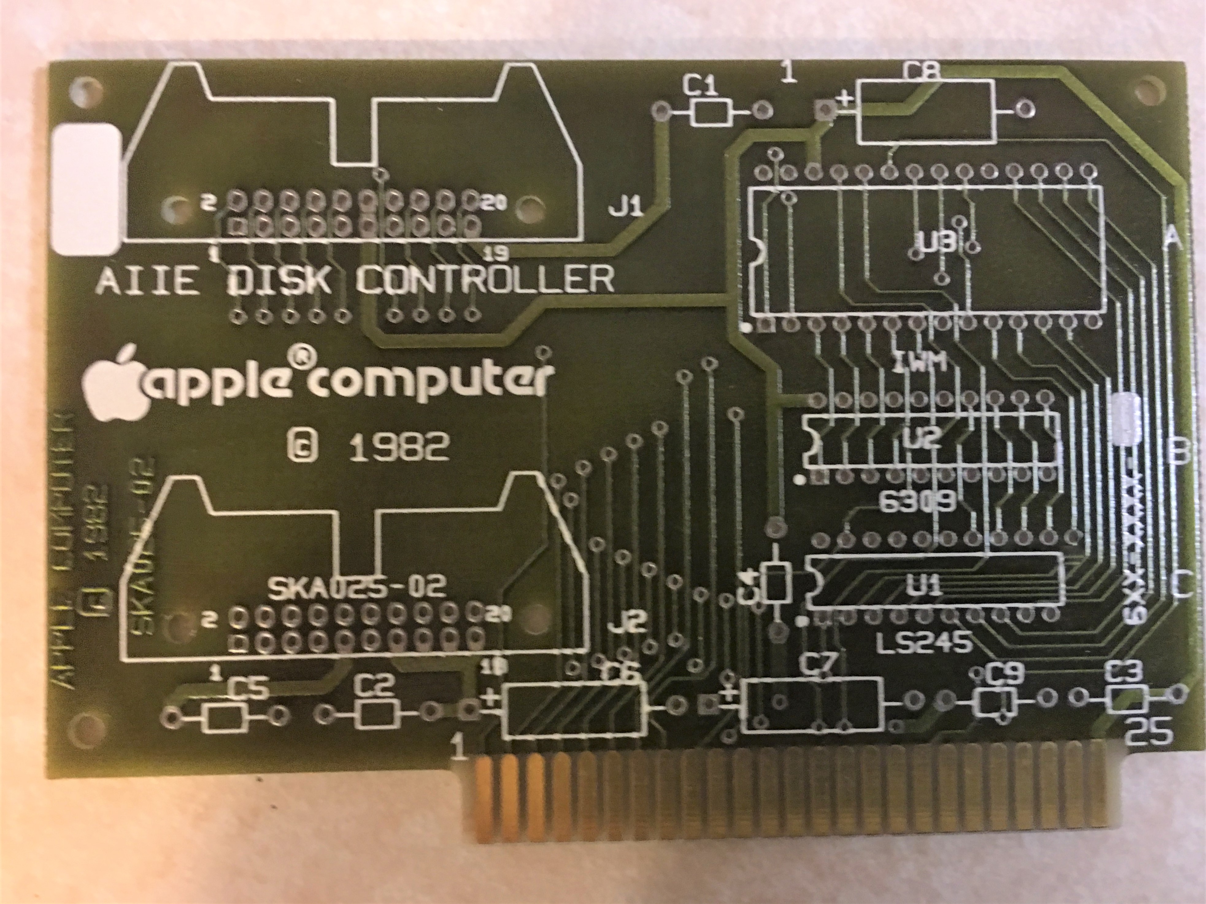
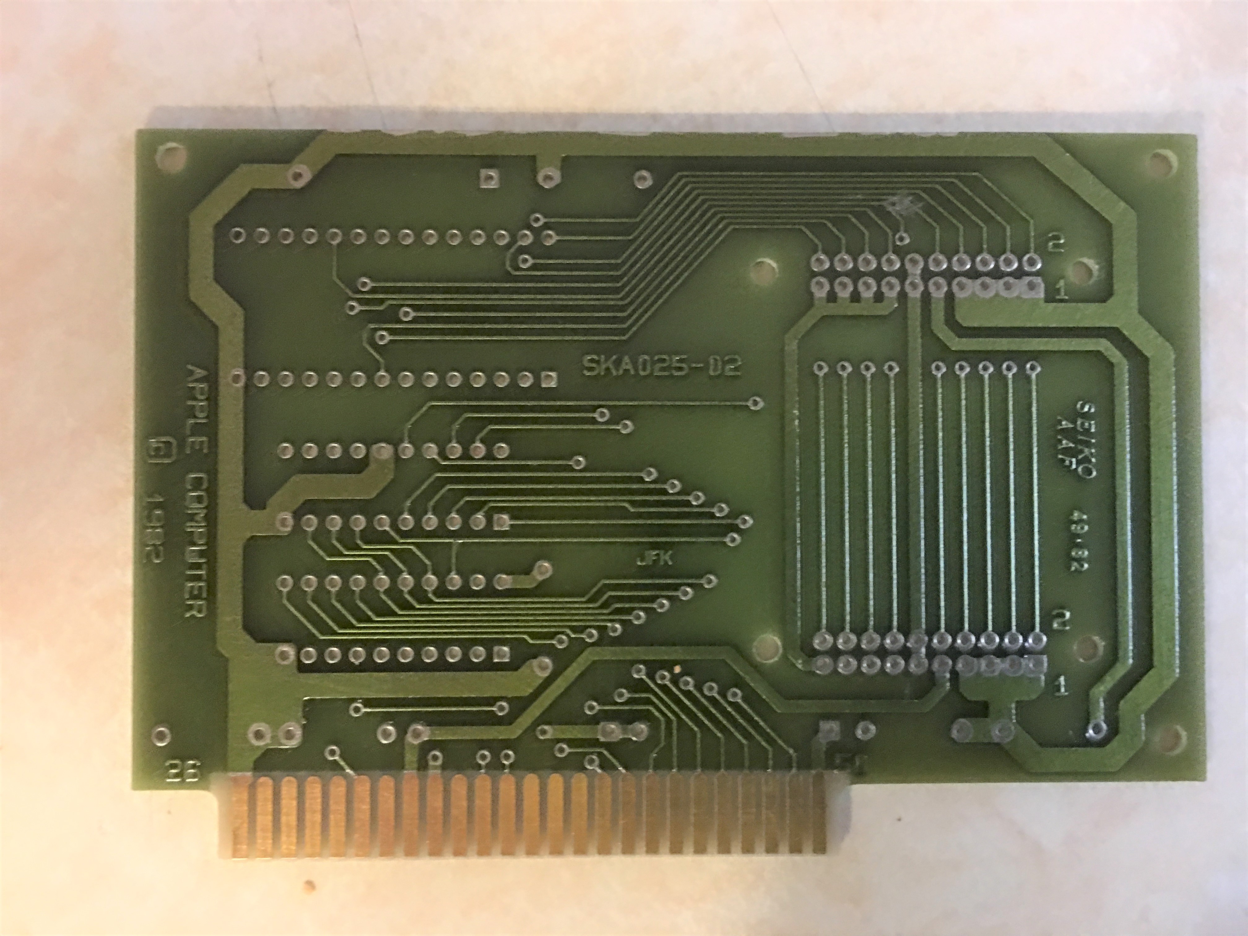
I just wanted to share what I found mixed in with a bunch of blank prototype boards. It's not the Disk II IWM card. At least not the one I have seen a photo of. This does almost look like a mirror image of that card. It says "AIIE Controller" deosn't have a part number, so I am guessing this was some kind of prototype card that never was. I have a collection of blank PCBs from Apple, but not one like this until now.
If anyone here on AF has any more info about it, let me know. I am going to post it on facebook too.
Thanks,
Jay
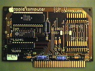
I included the IWM Disk II controller pic from APPLE2.ORG for reference.
Aha!
Your picture of the unpopulated board makes it possible to trace the route of pin 18 (R/W) from the edge connector to pin 1 (DIR) on the LS245.
AIIE DISK CONTROLLER.jpg
If you're familiar with circuit design in general then this probably seems like a perfectly-logical connection: the bus uses the R/W signal to determine the direction of data, so you might naturally expect a disk controller to be connected to that signal. But let's review the 5.25" devices Apple actually released...
In short, there doesn't seem to be any connection to the R/W signal in the devices Apple put into production.
I sure wish someone had called this to my attention back in the 80's when I was learning to program the Disk ][. Just guessing at this point, but I think this missing wire is linked to the bizarre limitation that an original Apple Disk ][ controller won't let you write to a disk by writing directly to the output port using
STA $C0EDinstead of the traditional method of using aSTA $C08D,Xinstruction while X=$60. On original Disk ][ hardware, writing directly withSTA $C0EDcauses the controller to record some bizarre constant, not the value from the accumulator.So that fits with the circuit description from Understanding The Apple II page 9-22 (boldface from original):
This probably explains why you can use
STA $C0EDon Micro-Sci, Franklin, or Laser disk controllers, which are just a teensy bit more forgiving than Apple's hardware. These third-party designs use a more conventional approach that latches data in response to bus signals (including R/W) but they require more than twice as many components! (In case you've never programmed the Disk ][ directly, it's brutally-strict about when and how your program sends data over the bus. If your program is 1-cycle-early or 1-cycle-late, Apple's controller will write an apparently-random value, whereas a third-party controller will just write the correct value with slightly-incorrect timing.)You are correct, the Disk II never needs a write signal as such. All "soft switches" activated by the address lines do not need to know if it's a read or write cycle. They work in either one, in the same way. As far as the "write data byte" going to the floppy disk is concerned, the Woz Machine just grabs any byte from the data bus which just happens to be there and loads it into the 74LS323 shift register when in the appropriate state.
However you have missed a fine point. The Woz Machine must be switched from SHIFT to LOAD mode just before the data byte is presented to it. This is done by the "phantom read cycle" of the STA abs,x which on the 6502 happens just before the write cycle. The designers of the 6502 put that in to avoid bogus writes ending up in the wrong place in case of page crossings. In instruction cycle #4, the 6502 does not have the correct address yet (with the carry over caused by ADL+X) so they decided to do one phantom read cycle in cycle #4 (with the ADH as per instruction byte / cycle #3 and no carry added yet) and then the write with the correct address including the carry into ADH is done in cycle #5.
Every STA abs,x to the Woz machine must be followed by a LDA abs,x immediately after the STA abs,x where the address of the LDA is chosen such that the Woz machine is changed back from LOAD to SHIFT mode. So that the next bit can be shifted out to the WR_DATA line when it is due. This happens juuuust in time. There is no leeway.
This is a very elegant and genius concept exploiting a "dirt effect" of the 6502 to reduce chip count by avoiding a pipeline register. Which needs not only said register, but also its control logic. This explains why the non-patent-infringing disk controllers all had to have so many TTL packages more.
A NOTE ON PATENTS (AVOID !)
But as to patents, the Taiwanese clone makers did not care. They stole Woz' design verbatim. This parasitic behaviour is seen up to today. They just make a shell company in China (i.e. HongKong) and "sell" the patent infringing product to that shell company, which acts as the exporter. Once the patent infringement is discovered, and a court has issued a "cease and desist" to the importer, the shell company disappears / is deregistred and liquidated and has no assets anymore. The original manufacturer says he is innocent, only having sold the product to another company in the jurisdiction of China. Sueing a Chinese company for patent infrigement in a Chinese court is futile ... good luck with that. If you even have a Chinese patent.
The bottom line here is that taking out patents is a total waste of time and money. Large corporations do it from time to time to have ammo for patent infringement lawsuits (What ? You sued us to infringe your patent #1233455 ? See how we counter-sue that you infringe upon at least one of our ten gazillion patents, and let's see in court which ones stick). This is why patent litigation never ends with a "winner". Except for the lawyers of both sides which laugh all the way to the bank. Typically, these lawsuits are settled out of court and sometimes end in a cross-licensing agreement. Which the "managers" then communicate to their designers in a hushed voice ... look at this nice patent of the competition ... you can use it in the product you design right now ... but don't tell anyone).
So if you have a cool invention, don't even think to file for a patent. Keep it as a trade secret and make a product based on it and sell it yourself. Pocket all the profit you can grab. When the competition has figured out how it works, it's technically obsolete anyways (in most cases) and you have grabbed all the money you could make. None of which went to parasitic patent lawyers or the USPTO. But never, ever disclose to anyone how it works. Not a peep ! Patents require such a disclosure and anyone, all over the world, who reads your patent (once published) gets educated on your dime. Don't do that !
If Woz had only waited till mid 1978 and had he then put the Woz machine into a brand-new PAL16R4 (or R6, or R8) from MMI with the security fuse blown, and otherwise kept his mouth shut, then it would have taken the copycats many, many years until they could have figured out how it works. (I am of course aware of the fact that MMI had terrible production problems with the early PALs ... so far could not figure out why, their PROMs did work, so why the problems with the PALs ?)
Hope you enjoyed my lecture.
- Uncle Bernie
If the disk II interface is not even connected to the R/W signal, it has no way of telling if the 6502 is truly reading or writing... What happens when someone kept writing to an address of the card's read register? Could I briefly cause the mainboard's 74245 bus transceiver and the disk II interface's 74323 latch to attempt to drive the data bus at the same time?
Yes. indeed you could.
In fact, you can cause that bus conflict by writing to any even-numbered IO port address on the Disk II.
So the instruction
STA $C088,Xboth turns off the disk drive and causes the controller to store the data register onto the bus at the same time the CPU attempts to store the accumulator onto the data bus. That's because address $C088 turns off the drive and because the controller's even-numbered addresses always read the data register.Conversely, you should be able to trick the Disk II controller into storing data that you never even wrote into the data bus. I will try to construct a routine that looks as though it should write
D5 AA 96, and really does writeD5 AA 96on a clone like Micro-Sci's A2 disk controller. But if the physical disk controller is a Disk II or IWM, it should write a different pattern,D6 AA 95as if by magic. (I'm confident this is feasible because I've tested each of the individual sub-components -- I just haven't pieced the whole thing together yet.)I've never seen even a picture of this card before. I wonder why Apple never produced it? You'd think that it would be cheaper to make than the Disk ][ Comtroller card or even the Apple 5.25 Controller card (DB19). I really wonder why they produced the latter card instead of something like this adapted for DB19. It would have made more sense with what they were doing with the //c. Also why they kept with the older designs by the time the IIgs came out in 1986. It would be interesting if someone came out with a GAL/CPLD/FPGA based IWM replacement and made a version of this card. Or possibly even more interesting, one with something like a 28C64 EEPROM with enough room to put the boot ROM and the LiRONGP code on it. Could be a cheap Yellowstone alternative (or alternative in general if Steve at BMOW isn't able to make more of those in the future).
A question for Uncle Bernie... Do you think making a replacement for the IWM with a 28 pin carrier with a couple of SOIC package GALs like ATF750C would be possible? It seems like the understanding of this chip and the basic Disk ][ controller cards is well understood enough that soneone who knew .pdl coding well enough could do it. I'm trying to learn that so I can create my own GALs but I'm nowhere near there yet.
In post #7, softwarejanitor asked:
"A question for Uncle Bernie... Do you think making a replacement for the IWM with a 28 pin carrier with a couple of SOIC package GALs like ATF750C would be possible ?"
Uncle Bernie answers:
I have a implementation of the Woz Machine in a single GAL16V8 (which could be a PAL16R6 of 1978), see here:
https://www.applefritter.com/content/uncle-bernies-woz-machine-based-apple-1-floppy-disk-controller
It's state machine equivalent to the original Woz Machine in the Disk II controller card but there were some slight modifications in the timing to allow use of the 74LS299 in lieu of the 74LS323 which is hard to find nowadays. From the software standpoint it's exactly the same as the original Woz Machine although I did not try it in an Apple II yet. The 74LS74 is just there for the RD_DATA synchronization and the two samples which are used to discern if there was a read pulse from the floppy disk. In the original Disk II controller these two flipflops are in the 74LS174 (which has 6 DFFs).
The "TFC" or "Time Flux Compensator" is a twist for the Apple-1 which became necessary because of the non-transparent DRAM refresh cycles in the Apple-1. Four of which happen within each 65 CPU cycles and so there is absolutely no way to compensate for that by software (do the math, you want exactly 32 or 40 cycles in the write loops).
Alas, I don't know anything about the IWM other than the scan of its spec sheet you can find as a pdf on the web. This spec is incomplete and many of the inner workings have been omitted. Wendell Sander should know more about it.
But I think that the whole IWM could be implemented nowadays with a small CPLD and if using the right small SMD package it would fit onto a PCB that would not be larger than the IWM DIL-28. The 10 macrocells in the 750C are not enough for the whole thing, though. You need to find a small CPLD or FPGA which has enough flipflops. These exist and are cheap but they come in super nasty BGA packages no hobbyist can ever solder. And they may need an extra regulator for the core voltage and in general, the 5V compatibility may be problematic. It's not so much the logic levels (a 3.3V part can drive TTL) but all the 5V logic around it trying to kill it.
But like all the grand and not-so-grand schemes with putting long obsolete designs in modern programmable logic ICs, the question is: it is worth doing ? I did that work just because after almost 40 years of my life pondering over the Disk II design I had to prove to myself that I finally had fully understood how it works. And such a proof is only valid if you build it. The non-transparent DRAM refresh of the Apple-1 was a mere nuisance which required one more GAL and a re-write of the RWTS to do all timed loops in 4 CPU cycles less.
- Uncle Bernie
One reason for putting the IWM into a programmable logic chip implementation is to offer a replacement for unobtanium parts to repair machines like //c, IIgs or early Macs if their IWM fails. Also it would be interesting to make the card that is the subject of this thread a reality, just for the sake of doing it...
Anyway, I figured a single ATF750C wouldn't have enough cells to do a full IWM, but if you use the SOIC package I think you could fit two of them onto a 28 pin DIP size package. I'm not sure if that would still be enough... As I said, I've got a lot to learn about these programmable logic chips.
Actually the chips that REALLY need to be reproduced like this are the //e MMU and IOU chips.
In post #9, softwarejanitor wrote:
"... unobtanium parts to repair machines like //c, IIgs or early Macs if their IWM fails."
Uncle Bernie agrees !
I have three Apple IIc and at least one has a fried IWM which typically happens when the internal floppy disk drive does not work and then some idiot tries to plug in a standard Disk II drive to see if it's the floppy disk drive or the IWM. Well, after that exercise it's certainly the IWM which is dead.
As for the MMU and IOU chips, these have a fairly trivial functionality and could be easily implemented in a bunch of early PLDs or GALs. I prefer the GALs because they are reprogrammable and I happen to have thousands of them. I happend to work on a GAL based reimplementation of the Apple II when I foolishly was sucked into the Apple-1 microcosm. After my last Apple-1 kit is sold, I will continue to work on this Apple II ("GALAPPLE") project but now I'm inclined to add some more skullduggery to make it switchable between Apple II and Apple-1 mode. But as with all of my projects, don't hold your breath. I do this as a hobby and have other interests, too. Sometimes these projects take ages ... like that Woz Machine re-implementation, which took me about 40 years to finally build it.
- Uncle Bernie
Here's what I would love to see... A two GAL implementation of the IWM... ATF750C if necessary but if it could be done with two GAL22V10 or two ATF16V8 that would be even better since those are cheaper and easier to find. With that a card based on this one using a 74LS245 and instead of the 6309 PROM, a 28C64 EEPROM with the normal boot ROM in the lower 256 bytes and the LironGP code in the rest of the ROM, as well as a jumper for "clipping" pin 12 (for safety using FloppyEmu as a SmartPort device).
I think that a card designed like this could be a pretty versitile disk controller and built and sold for around $50...
So I was just linked to this thread and... well, as it happens, I just completed the first revision of a CPLD-based IWM implementation, which I call TashMachine. (Not GAL-based, but beggars can't be choosers.) Here's the repo: https://github.com/lampmerchant/tashmachine
It's early days yet, I've only tested it on the Mac (the case with all the mode bits set) and I could use some assistance with the Apple II side of things. I've studied the Disk II chapter of Understanding the Apple II, but other than that I'm pretty much a total noob where Apple IIs are concerned - my interest is in Macs. I'd like to see TashMachine used in an open source clone of the Yellowstone card or something in that general vicinity, but I don't know what goes into that card other than an IWM - like, what sets it apart from a Liron card, and what sets a Liron card apart from an OG Disk II card... is it just an IWM attached to the bus with a special boot ROM, or is it more than that?
In post #13, 'tashtari' wrote:
" It's early days yet, I've only tested it on the Mac (the case with all the mode bits set) and I could use some assistance with the Apple II side of things. "
Uncle Bernie comments:
Seems you have approached the IWM substitute issue from the "other side", the Mac. For my 'IWMless' project, I approached from the Apple II side - simply because I have no Mac, and no Apple IIgs, so I could not test the FAST mode of the IWM anyways. The project thread is here:
https://www.applefritter.com/content/announcing-iwmless-iwm-substitution-call-beta-testers
The Apple II runs the 6502 at only 1 Mhz, which is too slow for FAST mode, although I could imagine some extremely memory consuming code based on an "unrolled loop" to handle the FAST mode data rate. A better way would be to use the RDY line of the 6502 to halt it when it read the IWM data register in FAST mode, and to release the RDY when the MSB is set (disk byte complete). This would eliminate the polling loop for testing for MSB being set. Which otherwise would be required both in the SYNC and the ASYNC modes of the IWM. I mention this only to show the way how Apple II could handle FAST mode, and this would allow it to read / write Mac formatted diskettes without adding an extra 6502 CPU running at 2 Mhz (or more).
To turn your "tashmachine" into a IWM substitute being able to work with the Apple II, all you need to do is to provide two further modes:
- the SLOW mode (/FAST) where the time duration of all the bit cells are doubled both for read and write. But for the ASYNC mode, you still need be quick with the handling of the MSB, so you can't just divide all the clocks by 2.
- the SYNC mode in which the IWM reverts to a behaviour resembling the 'Woz Machine' in the DISK II.
What I did is that I first implemented the ASYNC + SLOW mode and then update the output data hold register all the time (at each bit cells) if in SYNC mode, while changing the MSB handling slightly, which differs from the "Woz Machine" when the IWM is in ASYNC mode.
What I can guarantee to you is that if you try to implement this: you will run into lots of trouble with weird tricks the Apple II "SmartPort" functions play with the IWM. It took me months to analyze all the ways "SmartPort" could crash or hang. The best test bench for that is to run 'TOTAL REPLAY' on an Apple IIe equipped with a fake 'Liron' card in which the IWM is replaced by your CPLD. This runs in automatic demo mode. And if it hangs in any place other then 'SERPENTINE' - which hangs under certain conditions even with the original IWM - then your implementation is not perfect. There is a thread here on Applefritter about the 'SERPENTINE' problem. If it could be removed from "TOTAL REPLAY" then you would have a perfect test bench for your IWM substitute.
The only question you should ask yourself is whether it's worth your time to do this. For fixing Apple IIc and 'Liron' cards, my 'IWMless' was developed, and its development is complete, although it is still in beta test (it takes time to test the 3500+ software titles available for the Apple II in copy protected form).
The only demand for your work outside of the Mac realm which you have covered already would be the Apple IIgs and the currently viable procedure to fix those IIgs with dead IWM is to salvage an original DIL-28 IWM from any Apple II related parts donor, put it on an adapter, solder that adapter into the IIgs, and then use an 'IWMless' to make the parts donor whole. If you get your work to be a 100% compatible IWM substitute, then you can avoid the parts donor, but you will still need an adapter to match the footprint.
As for replacing the 'YELLOWSTONE' card, I don't think this is worthwhile to do. It is a fine and reasonably priced product for those who need all the features it provides. This is a small minority of Apple II users. I think that most 'YELLOWSTONE' users only use it as a 'Liron' card replacement and never use the other features it offers. I have made three (!) 'Liron' card replacements based on the 'IWMless' and that covered all the demand/need for that solution.
Draw your own conclusions. The Apple II retro computing realm is much, much smaller than you might think. The Apple-1 retro computing realm is even smaller than that (only < 1000 people worldwide). So is it worth doing what you propose ? I don't know. But IMHO Applefritter is the right forum to find out. I post all my projects here and the demand (or lack thereof) created by these postings saved me a lot of time by NOT designing PCBs for my projects for which only 2-3 people worldwide showed interest. For me, these my projects are fun even when they don't generate interest / adopters and I'm totally indifferent to that fact, as I design these things for myself, to prevent brain rot / losing my engineering skills. What I really would hate is if I designed PCB layouts for these projects just to find out nobody adopts them - these 2-3 people who have shown interest don't justify this expense of my time. If it was 20-30 people, I'd do a PCB layout and give it away. I never had profit interests with any of my projects (if I could make $1 Million per year in profits, that would really make me greedy and I'd want to do it, but anything less is simply 'peanuts' - not worth the effort needed to cut through the "read tape" foisted on us by useless, unproductive bureaucrats, so a profit-less hobby it must be - read 'ATLAS SHRUGGED' to understand how the world really works and how I tick - but be warned it's fraught with unnecessary drivel on romantic relationships only a woman can write, but her philosophy about the motives of running any enterprise and how government meddling hinders that is right on the spot).
- Uncle Bernie
Interesting stuff, I was not aware of the IWMless project before now, and I salute your thoroughness and attention to detail.
TashMachine actually already has support for all five IWM mode bits, including fast/slow mode and async/sync mode - though, as I said, I haven't yet production-tested any combination of them other than the Macintosh's all-ones configuration (due to lack of Apple II machines in which to do so). I did my best to implement the other modes according to the IWM datasheet and testing I've done with my rudimentary test bed suggests that they work as I intend them to, though of course that only means so much, especially if SmartPort devices are as finicky as they sound...
As to what's worth my time, that's a complicated question. In the nearer term, the most important thing to me is providing an IWM clone that can be used with Mac Plus/512k/128k and non-FDHD Mac SE machines. I'm willing to put in some effort to make the Apple II modes work as well (up to and including the functionality used by the IIgs) and support the creation of cards that use its capabilities to the fullest, but this may prove to be beyond my reach. In the longer term, I envision that the only retrocomputing that survives is going to be that which is in the form of data - that is, that we're going to wind up replacing more and more of our retro computers with newly manufactured programmable logic devices of various kinds - and therefore I'd like to do my part to make sure that by the time that happens, there's a mature HDL implementation of the IWM that can slot easily into any Apple- (or Mac-) in-an-FPGA project.
Whatever the case, I do this for fun. Practicality is negotiable and profit is of no consideration at all. =)
Tash, you're the best. Just when I was looking for this exact thing.
I'd love to work with you on an Apple II card.
I'd be glad to work with you, but the news of UncleBernie's having already done the work with IWMless (and having a full IWM clone in the wings) makes me wonder if it's worth doing...
@UncleBernie What are your plans with regard to the full IWM clone that you mentioned?