Hello everyone, I have recently found my old Apple IIe computer in my father's garage. That led me down a rabbit hole and I am now trying to understand the schematics of the MMU.
These:
Apple IIe - Schematic - MMU Logic - 1 of 2
and
Apple IIe - Schematic - MMU Logic - 2 of 2
These schematics seem to be official Apple documents and they are dated Feb. 1983 -- after the Apple IIe's release. So, they are probably very close to the final MMU design.These schematics also probably went through multiple iterations and verifications and should be free of obvious errors.
Yet, there is something really weird behind the logic for the evaluation of INH' (located near C-2 of "MMU Logic 2 of 2", middle right). I'm probably missing something, but all the logic behind and up to the component L8 is ignored.
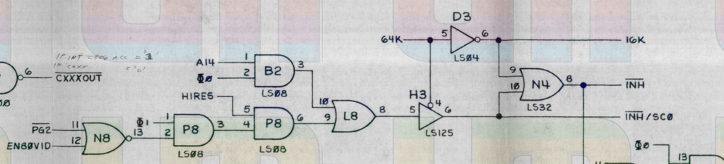
-If 64K is HIGH, H3-6 will be high-impedance and the value of INH'/SC0 (an input on the MMU, pin 15) will be used.
-If 64K is LOW, H3-6 will be the result of all the logic behind, but it doesn't matter since the N4-9 pin of the OR gate will be HIGH.
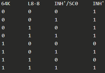
Truth table for this:
There is another schematic for the MMU, maybe that one could help us understand:
This one is much harder to read, but it is really fantastic to look at -- to think all this was drawn and designed by hand!As a hobbyist, it's difficult to know if my understanding of it is wrong (it most probably is).This is what I understand of it's implementation of INH'
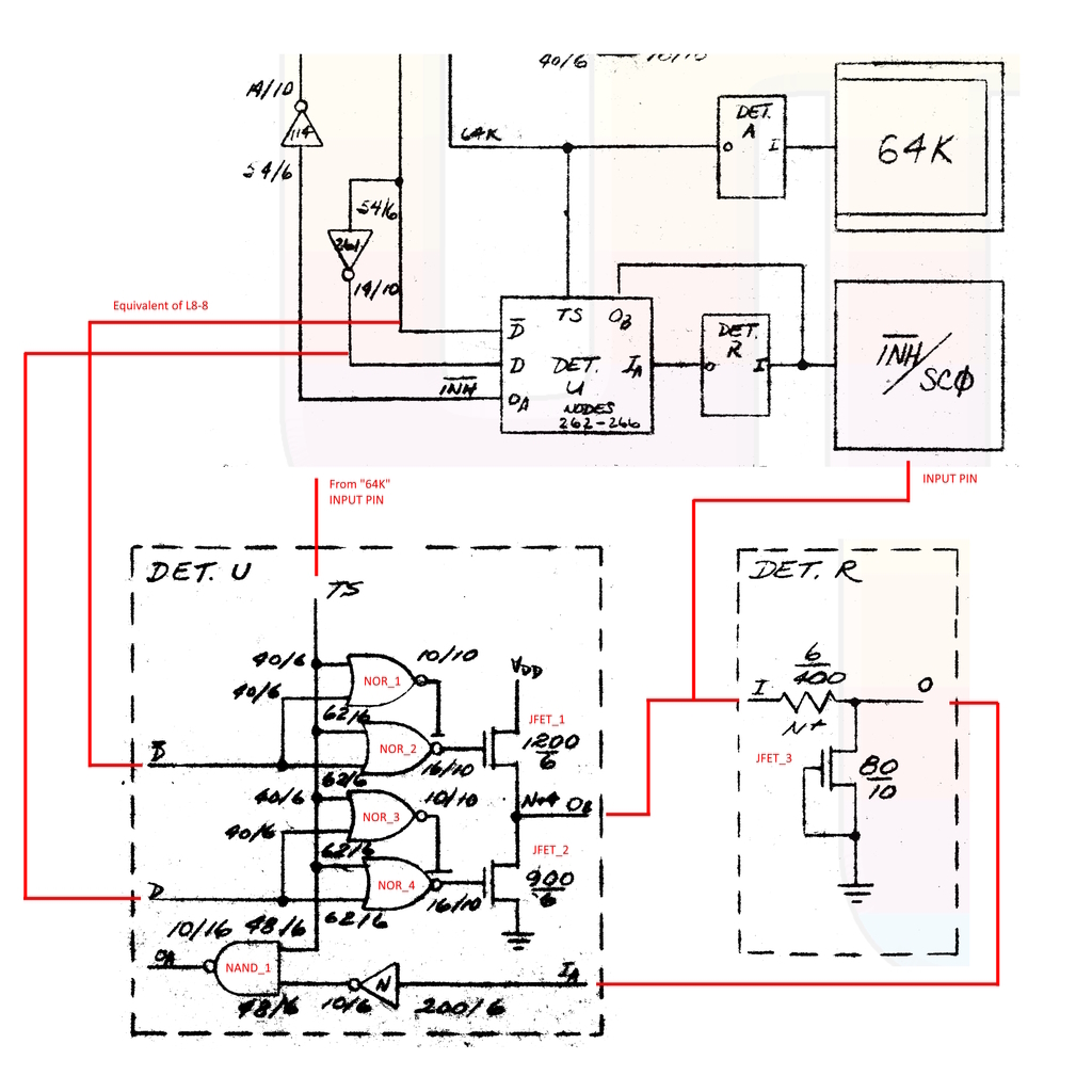
There are two pairs of NOR gates NOR_1 and NOR_2 in the top-middle, and NOR_3 and NOR_4 below. Both NORs in a pair have the same inputs, but the top NOR of the pair seems to be an enable/disable for the other NOR. (I have never seen such a notation on the NOR output before but again, I'm an amateur)
The output of the pair can be HIGH or High-Impedence, and the two pairs operate one the inverse of the other.
Since a JFETs will block current if it's gate is HIGH and allow current if it's gate is High-Impedence, this is what I think Ob will be:
The input of DET.R is connected to both Ob of DET.U and INH'/SC0. I'm not sure exactly what DET.R does but I think it function similar to a pull-down resistor. So IA of DET.U will HIGH if Ob or INH'/SC0 is HIGH.
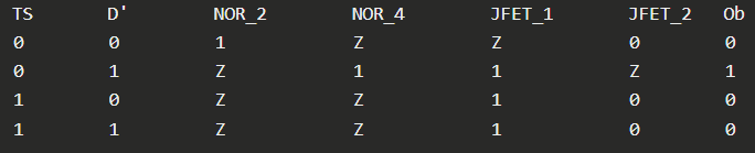
Merging everything gives this truth table:
We get the same values for INH' in both schematics. That can't be right because in both cases, INH' can be simplified to:
(not 64K) or (64K and INH'/SC0)
We don't need L8!
I'd be grateful if someone could tell me where I'm wrong.
I've been hoping for a long time that someone will develop a CPLD or FPGA based replacement for the //e MMU (and also the IOU) chip. These parts are getting hard to find. They are basically the only parts that currently would prevent the ability to build a more or less new //e from scratch like can be done with a ][+.
I don't think pin 15 on the MMU is just an input. In the Apple IIe it's being pulled up by a 3.3k resistor that is part of the RP1 matrix, so if 64K is low, pin 15 of the MMU will be whatever comes into H3.
That isn't the circuit symbol for a JFET, and JFETs were not used to make LSI logic chips. Those are MOSFETs.
To understand the function of the circuit, you need to pay attention to those "40/6" figures. They weren't written in for the hell of it. Those numbers specify the width and length of each transistor's channel. The notation is "width over length" because that is proportional to transconductance (g). On a broad view you can think of g as the "strength" of each channel when in the conducting state.
Because the gate of a MOSFET normally has no connection to its drain or source, it acts as a capacitor: once charged high, it will stay high until it is discharged low. So "high impedance" inputs do not switch the transistor on or off, but leave it in its previous state. This implies that your understanding that
must be incorrect, because it would leave both the high-side and low-side FETs switched on at the same time, causing shoot-thru and destruction of the chip.
Looking at "DET. R" is also interesting because it deploys a channel without a gate as a resistor (with a channel length far greater than width), and another FET as a capacitor (with its gate connected to its source, it will be "off" forever and just act as a capacitance). This produces a R-C delay between the input and output of that block, so when the signal feeds back into IA, it is ANDed with a different TS than before. I think this logic means that inhibit is true (logic low) when TS transitions from low to high after D or the /INH/SC0 input has been low.
This makes me seriously question the many voices on the web that expressed the opinion that the IIe ASICs can be "trivially" implemented in FPGA. There is clearly more than synchronous logic there.
Forget the second schematic, but the first one seems to be of an emulator for the MMU chip built with standard TTL chips. Has anyone tried to build it and see if it works? Maybe a full length extension card with a ribbon cable that plugs into the MMU's socket.
If you search mentions of INHIBIT' in this book:
Understanding the Apple IIe
It seems to be an input only pin. Plus, according to the complete MMU schematics, it also seems to be an input only pin.
Thanks robespierre, understanding this schematic will be much more difficult than I though. Two things though:
One, I think the 64K line is not really a 'signal'; it is labeled a 'bonding option'. I think it's value is 'hard-wired' in the ASIC because if you look at the other bonding option, it's called DIANA which was one of the codenames for the Apple IIe. All this to say that it is possible that the TS input is hard-wired HIGH or LOW.
And two, CVT is right. I *has* been done. I can't seem to find it but I remember seeing a photo on the internet of the prototype of the MMU and IOU all done entirely with TTL chips by Apple engineers before the IIe was released. An impressive board of chips but that shows that if there are async effects in the MMU, they are not essential.
In post #4 Robespierre wrote:
"Looking at "DET. R" is also interesting because it deploys a channel without a gate as a resistor (with a channel length far greater than width), and another FET as a capacitor (with its gate connected to its source, it will be "off" forever and just act as a capacitance). This produces a R-C delay between the input and output of that block, so when the signal feeds back into IA, it is ANDed with a different TS than before. I think this logic means that inhibit is true (logic low) when TS transitions from low to high after D or the /INH/SC0 input has been low."
"This makes me seriously question the many voices on the web that expressed the opinion that the IIe ASICs can be "trivially" implemented in FPGA. There is clearly more than synchronous logic there."
Uncle Bernie comments:
DET.R is not a RC delay circuit (the grounded gate turns the transistor off, no channel formed, almost no capacitance). Instead, it's the classic ESD protection structure used in NMOS technologies. For the sake of understanding the logic, you can ignore it and replace it with a direct connection from the pad to the inputs of the logic gates.
The third link of post#1 is a very poor quality scan of a schematic - all I can decipher from it is that the circuit design was done by SYNERTEK targeting their NMOS depletion load process (same process as for the 6502). I think there is some dynamic logic inside although it's such an eyesore I don't want to dig into it any deeper. This can be tricky to implement in an FPGA - you can't do it directly. All the dynamic storage nodes need to be replaced with a register. If there are precharged bus lines which get conditionally discharged by more than one gate, it gets even more tricky. But tools have been written to take a transistor level (SPICE) netlist, automatically analyze it, and then generate Verilog code which mimicks the logic. This Verilog then can be re-synthesized to full custom CMOS or FPGA or whatever. It has been done for the 6502, based on the netlist from the visual 6502 project (www.visual6502.org). And the 6502 has many foul dynamic logic tricks and precharged busses inside. So it can be done. If you have an accurate SPICE netlist. We we don't have (yet) for the MMU or the IOU.
"CVT" in post #5 is right, the first two links point to schematics for TTL based "breadboards" which emulate the desired functions of the planned full custom IC. This was the standard method back in the day. Expecially when replacing existing logic with a custom or semicustom IC. You had to build that "breadboard" which then plugged into the target system. And surprise, surprise - in most cases it did not work at the first power up despite the "breadboard" was 100% the same function of the datasheet(s) of the ICs to be substituted. And then the ICE and the Logic Analyzer where thrown into the battle. The root cause found often was some timing bug in the target system violating the datasheet spec, or the programmer of the code in that target system had "exploited" some undocumented feature of the IC(s) to be substituted. Been there, done that. Since I used PLDs (later: GALs) for my "breadboards" the fix was quick, and after a few iterations everything worked and the customer signed the design off to be cast into a full custom or semicustom IC (aka "gate array"). The advantage of using PLDs was that their source equations could be automatically translated to the form needed to feed the (often proprietary) CAD system of the semiconductor manufacturer.
This said, based on my own professional background, I think the most efficient route to get to a MMU into a FPGA would be to first analyze their "emulator" / "breadboard" circuit and put it into a few GALs. Then build it an plug it into the Apple IIe. Once it works and is debugged, you can then put the PLD equations into an FPGA.
Why not using an FPGA from the beginning ? The reason is, it is much harder to debug together with the target system (the Apple IIe). If you want to hunt a bug down you need access to one or more inner nodes of the logic. With FPGAs you can route inner nodes to pins and attach a Logic Analyzer there, but this is much more time consuming than in case with the (simpler) PLDs where every node is readily accessible on a pin (don't use PLDs with buried registers). Furthermore, any change to the FPGA to route inner signals to pins causes re-fitting of the logic and problems may mysteriously go away or new ones may appear. Despite the actual, active logic should have stayed the same. Only if you start with a "clean slate" design where you don't need to fight unknowns in strange logic made by other persons (in this case, decades earlier), you would use FPGA from the beginning. Because then, you can develop, simulate and the test the FPGA stand alone and then everybody downstream must make their stuff work with your FPGA. This is a completely different situation. Of course, opinions differ and some FPGA offer better ways to probe internal nodes but I found if the function can be done with half a dozen to a whole dozen simple PLDs, then using them for the initial debugging of such substitution projects is quicker and more painless than using FPGAs. I know of cases where designers have used FPGAs and failed to deliver the substitute and then the customer came to us and we did it with PLDs, in two weeks, while the FPGA attempt had wasted months. Typically, these FPGA failures involved those surprising quirks in the hardware and/or software of the target system. I can only imagine how desperate this FPGA designer got when he had two "black boxes" with dubious contents - the target system and his FPGA. Because yet another complication with FPGAs is that the actual logic inside is NOT the logic you wrote in the HDL. This can lead to nasty surprises every time you press the "re-synthesize" and "fitter" button. Only when ALL aspects of the design work to do are fully known and documented ("clean slate" design), FPGAs reign supreme. Otherwise they are a PITA. Take this as a warning. Hobbyists have wasted years of their life trying to re-implement vintage, poorly documented functions in FPGA based "replica" machines. And never arrived at a 100% perfect substitute. And never found out where the differences come from. So, for certain missions, it may be better to dial back the level of technology used to get results quicker.
- Uncle Bernie
Uncle Bernie, your post was the perfect read for a friday evening.
I was a young kid in the early 80s when the Apple IIe came out. And to borrow the words of a wise old man: "I am old enough to have witnessed a lot of 'first times'". I have witnessed the 'first time' people realized computers could be a household item. I read your post and I think you lived through the golden age of hardware development; mature enough to be undertood but still so much to explore and discover. Reading the schematics and books of that era makes me realize how a magical this time must have been. "Anemoia" is probably the correct word.
As for the weird INH' signal, we're fortunate enough to have lots of books written on the Apple IIe. I want to design something as close as possible to the original, but if that's not possible at least the behavior from the outside is well documented. Plus, the Apple IIe is heavily inspired from the II+ and have heavily inspired the IIc. Two systems that are also well documented. And finally, we have AppleWin, an emulator that is very mature and can certainly help us understand the Apple IIe circuits.
In post #8, frozensignal wrote:
"Reading the schematics and books of that era makes me realize how a magical this time must have been."
Uncle Bernie comments:
Yes, these were the glorious 1970s. The birth of the microprocessor. I was there (played as a teen with the first ones, like 8080, and then the 6502) and later became a professional IC designer. One must-read book for true aficionados is:
Mead / Conway "Introduction to VLSI Systems"
These can be had very cheap ( ~ $15) on Ebay and from used book sellers. It's a wonderful book which explains NMOS depletion load dynamic logic design and how to make the layouts. The examples for that 16-bit processor on the cover the students of Prof. Carver Mead have designed have very pretty and clear layouts, although some aspects are ludicrous, such as using excessively long poly runs at some places. Lambda design rules also are area inefficient (although very easy to learn). Professionals didn't do that. But still, once you have understood what is in this book, you can go on the visual6502 web site and understand everything seen there. If you had the original 6502 schematics from MOS Technology, you could read them, too. There are not too many people in the world who have them.
It was a magical time indeed. And I can say that almost everybody who jumped onto that bandwagon back then (full custom IC design, first NMOS, then CMOS) had a very lucrative, rewarding, and satisfying career.
Most are retired now (like me) and have no regrets. We had a good run over 40-50 years. Now the whole semiconductor industry is losing momentum and process technologies have progressed to a point of diminishing returns at exploding costs, both to build these 5nm and below wafer fabs, and to design new products leveraging the powers and capabilities of these leading edge technologies. The problem, as I see it, is that there are not many product types / functions which a) require billions of transistors on a chip and b) can be sold by the 100's of millions before they get obsolete. In other words, they are hitting a wall. Diminishing returns on investment. The big players in the field with deep pockets (lots of $$$ or $$$ credit lines) hoovering up all the smaller players is one sign of that. Salaries for IC designers will fall, same thing what happened with automobile designers, and as a consequence the brighter minds will go elsewhere, towards other industries where the money fountains still are full open throttle. The inevitable consequence of this consolidation process (which happens to every industry once it reaches maturity) is that the products will become more and more dubious and crappy. You can see this already with some consumer products whose ICs obviously were designed by idiots who don't know the very foundations of what they are doing. As an example, cheap flat panel TVs now show a loss (or ignorance) of subtle know-how what IC designers for such functions still had back in the 1990s. Possibly designed by some rookie engineers somewhere in India or China who get the pay of a Walmart greeter and never have seen a real, analog TV in real life. Sure, analog TV is on the way out, but proper support of these legacy systems still should be there.
I think the complexity of and the frustration with these modern electronics is a key factor why more and more hobbyists (and retired professionals) return to the "good old days" where men were men, women were momen, and transistors were transistors. And where discrete components like resistors and capacitors did not look like what comes out of a pepper grinder.
Oh, the good ol' days !
I wish I had a time machine to travel back to 1978. It should also rejuvenate me by the same amount of years traveled. Oh, and of course I'd want to keep my knowledge of modern semiconductor technologies. I could become a real world Tony Stark. Alas, it's just a dream.
Good night !
- Uncle Bernie
I think I have a general idea of what this is. I was way off target it seems.
Thanks to "CVT"; you set me on the right path with your comment that pin 15 not being just an input pin. Initially, I though what if this pin is a bidirectional pin? But why then is it linked to the bonding options?
There is another pin that also use DET.U and DET.R (DMA'/C06X'). What is the link between DMA and C06X (cassette read and joystick input)? And in the pin INH'/SC0, what is SC0?
And finally, if these pins are bidirectional, why isn't it even mentionned in any book?
I started to understand when I tried (in the big MMU schematic) to find other circuit parts that looked similar to DET.U, but whose function were known. MD7 pin is very similar, and we know that it is an output pin. So, I believe that the TS line of DET.U must mean Toggle Switch and DET.U will be an input pin or an output pin depending on TS. And the name INH'/SC0 must mean that the pin will be an input INH' or an output SC0 depending what bonding option was selected at manufacture time. As for SC0, by examining what logic makes up L8 (signals related to the language card), SC0 must mean something like "Slot Connector 0".
We'll probably never know the history behind these input/output bonding options, but they were probably only used at some point during the development of the Apple IIe. And it is clear that no production MMU has these pins configured as outputs with C06X' and SC0. I haven't decided if I should include or exclude the "alternate" pins functions in the HDL code. We'll see.
Also, while searching on the internet I found a photo of the prototype made by Apple:
DISCRETEMMU+IOU.png
(Source: http://www.applelogic.org/files/DISCRETEMMU+IOU.png)
And these are actual delayered MMU and IOU photos:
MMU:
https://commons.wikimedia.org/wiki/File:344-0010_Apple_8314_cleaned_enh_med.jpg
https://commons.wikimedia.org/wiki/File:344-0010_Apple_8314_delayer_med.jpg
IOU:
https://commons.wikimedia.org/wiki/File:344-0020_Apple_8317_die_240nmpp.jpg
In post #10, frozensignal wrote:
"We'll probably never know the history behind these input/output bonding options, but they were probably only used at some point during the development of the Apple IIe. And it is clear that no production MMU has these pins configured as outputs with C06X' and SC0. "
Uncle Bernie comments:
I don't have the time to look into it, but nobody puts useless circuits on ICs. So there are only two possibilities what these "unused" inputs might do:
a) extra functionality which was foreseen for future Apple IId,e,f products but never used.
b) test functions for testing these ICs at their manufacturer.
It is quite common that ICs have pins / pads with undocumented test functions. To find out, analyze under which condition these pins turn into inputs. If that condition is "weird" (meaning: not useful in the target system or makes no sense from the viewpoint of the target system) then it's most likely a test function.
- Uncle Bernie
Haven't the first chips of a series been manually bonded into housings like this?http://www.syntezmicro.ru/uploads/images/service/5u6.jpg
5u6[1].jpg
So it shouldn't be a problem to use some 52 pin housing for the test chip and 44 or 48 pin for the final product.
Beside that the actual chip is larger than needed.
Also there have been a lot of strange IC hosings like the ones below, they would give a lot of possibilities to bond extra test pads:
https://www.cpu-world.com/CPUs/3870/Mostek-MK38P70-02%20(97400A).html
I had the opportunity to take a closer look at the scanned transistor level schematic (after I discovered how to open it with a tool that has magnification built in, it was readable).
So I could answer the questions above, but don't want to waste any of my RQLT on writing and posting the answers here if nobody reads them.
Found some functions in the MMU transistor level schematics which seem to be undocumented in the Apple IIe programming notes. There is a flipflop which controls the fate of the $C800-$CFFF page (ROM there or not) which can be flipped and flopped by any access to the $C3XX page and to the address $CFFF, if a certain soft switch is cleared (in its RESET state).
Does anyone know any documentation about this function ? It seems this function is missing from the TTL schematics of post #1.
- Uncle Bernie
I understand your time issues, however someone being able to build a modern PLD based replacement for the unobtanium MMU chip would be a great thing for the community. Documenting it here for posterity could possibly aid in that. I wish I had the expertise to do the work myself.
I believe frozen signal did end up building it, but he switched to this topic: Homemade MMU and IOU progress thread
as well as this blog: The first working(-ish) homemade MMU
Very impressive work I think.
Yeah, it looks like some progress has been made, but at this time nothing is available that other people can use. It's encouraging though. Those two chips are about the only things that prevent modern built //e motherboards from being possible.
Hello everyone,
>So I could answer the questions above, but don't want to waste any of my RQLT on writing and posting the answers here if nobody reads them.
Thanks Uncle Bernie for the offer! That won't be necessary, however. I apologize for not posting updates and progress on this site but, I've progressed a lot since that initial question. I've been working with Henry from ReactiveMicro (he's the one who made all the schematics available to the community!) since may to create a homebrewed replacement IOU and MMU. We are finalizing the IOU, and the MMU should follow shortly after. The sources for the MMU and IOU are on my github repository (https://github.com/frozen-signal/Apple_IIe_MMU_IOU). They are open source and I released them as Public Domain; anyone can do whatever he wants with them. I do not encourage to start a project with them right now, however; there are still a few problems with the IOU, and the MMU is developped but untested right now. I expect them to be fully functionnal in the near future. Eventually, I'd like to also write a guide to help the unitiated understand how to build a MMU / IOU from the sources, understand the schematics and maybe also document other miscellaneous infos like timing requirements.
So to return to the topic of the schematics, what we realized is that these schematics are solely for a TTL-based emulator that combines the MMU and the IOU. These schematics are mostly correct but, if implemented exactly, will not work or will not have the same behaviour as the ASIC MMU and IOU.
The mysterious logic that did not seem to be used is in fact logic that is used for the Apple IIc. I suppose it was more cost effective for Apple to create a single design and switch the bonding options to produce a batch for the Apple IIe or Apple IIc. The good news is that we will likely also be able to add the IIc features once the MMU and IOU are finished for the IIe.
Although I still can't read gates directly on a decapped die, I think I understand enough the ASIC schematics of the MMU now. The thing that puzzled me the most were notations like this:
Strange figure
Until I read the book you recommended higher in this thread (Introduction to VLSI systems) and spotted this on the schematics:
Fig2.png
I recognise pull-ups transistors on top, and a NOR gate modifed to be like a super-buffer. That would make sense since these kind of constructs are only seen near the pads. So, for the sake of understanding the schematics, I think that these are equivalent to a normal NOR gate.
>There is a flipflop which controls the fate of the $C800-$CFFF page (ROM there or not) which can be flipped and flopped by any access to the $C3XX page and to the address $CFFF, if a certain soft switch is cleared (in its RESET state).
I think I understand what you are refering to. In the MMU logic schematics, it is on the second MMU page, square C-4 (component F2). That is tied to the computation of ROMEN1'. This is not an undocumented feature; you can read what it does in "Understanding the Apple IIe" by Jim Sather, p.5-28
I'd take the opportunity to ask your opinion on something. Henry is currently designing the final version of the IOU. We'd like to add a way for anyone to be able to program his IOU (a CPLD, in case we discover a problem after release and/or to let users experiment with it). We are trying to find the best and smallest way to allow for JTAG. Henry proposed something like this (TC2030-IDC-NL):
JTAG.png
which looks really fantastic, but would likely require people to buy a cable. On the other hand we could go with a standard JTAG header, but fitting it on such a small PCB is not easy and doesn't look as good. I'd be grateful to have your thoughts on this, what do you think would be the best way to let people program their IOU/MMU?
All very good news. I wouldn't personally consider having to buy a cable or even a programming device to be a huge issue. I've got the tools for several of the CPLD/FPGA vendors, Xilinx, Altera and Lattice already.
I have a couple //e motherboards which would work except for bad MMU or IOU chips, so this development is extremely interesting.
In post #17, frozen signal wrote:
"I recognise pull-ups transistors on top, and a NOR gate modifed to be like a super-buffer. That would make sense since these kind of constructs are only seen near the pads. So, for the sake of understanding the schematics, I think that these are equivalent to a normal NOR gate."
Uncle Bernie comments:
Yes, these are superbuffers expressed as logic gates. So it was worth for you reading Mead/Conway. Just for those reading this thread and not having the book, superbuffers just use a top side NMOS transistor with an actively driven gate, while normal NMOS gates don't drive the gate on their top side NMOS. Top side NMOS means the pullup to VDD, of course. The advantage of the superbuffer is that the bottom side (pulldown) NMOS does not need to fight the top side NMOS, so more current is available to drive the load. It's not advised to have beefy transistors fighting each other anyways. For small static gates it doesn't matter much, although thousands of such static gates can make the die quite hot. The disadvantage of any super buffer is the extra logic to drive the top side gate. With CMOS these circuit tricks all went away, just use a PMOS on the top side and all is good. Just for completeness, the normal static gates use a depletion mode transistor whose gate is tied to the output of the gate as the pullup. Depletion implant just causes a threshold shift such that the top side transistor is always turned on, even if the gate is near circuit ground. Essentially, it acts as a pull up resistor. And all the gates with output "Low" on a chip fight all these pullups. Which wastes power and make the die hot.
In post #17, frozen signal wrote:
"I'd take the opportunity to ask your opinion on something. Henry is currently designing the final version of the IOU. We'd like to add a way for anyone to be able to program his IOU (a CPLD, in case we discover a problem after release and/or to let users experiment with it). We are trying to find the best and smallest way to allow for JTAG. Henry proposed something like this (TC2030-IDC-NL).
I'd be grateful to have your thoughts on this, what do you think would be the best way to let people program their IOU/MMU?"
Uncle Bernie answers:
Define what you mean with "best way". In Colorado Springs is a local trash hauling company who has that name. What I mean with this joke is that what is "best" depends on the user and not what you think is best. The industry would use that TC2030-IDC-NL connector without regret and just buy the $40 cable. Writing out the order for the cable might cost more than the cable itself. But the hobbyist will curse you if he is forced to by a cable which costs more (I guess) than the whole IOU CPLD card. What I would do is to have both the TC2030-IDC-NL footprint and six small pads into which a hobbyist can solder a few wires going to a 0.1" raster pin header (i.e. 2x3 pins), or, if space permits, have larger pads such that such a header can be directly soldered to the PCB, on some edge of it. This way, hobbyists could make a cheap programming cable all by themselves, with stuff found in a typical hobby electronics lab. Yet another concern is that weird special connectors tend to disappear over the decades, I got burned with the special 100 pin (IIRC) connector in the XILINX Spartan III board. Even back when these FPGAs were new, the connector (IIRC made by Hirose / Japan) was only available from one distributor, and at a heinous price. Fast forward 15 years or so and I could not get these connectors anymore.
A few other comments
I appreciate your project very much. I was working on an Apple IIe implementation in GALs since the mid 1980s, on and off, with decades of idleness in between, but never got anywhere near a completed Apple IIe replica based on them. Since I retired from my job as an IC designer, I have picked up my old abandoned projects again and I think the MMU can be done in 5 x GAL20V8 plus maybe 4 small TTLs. I have a similar low chip count implementation of the IOU, too, again based on GALs and some TTLs, except for the mouse functions. I don't intend to duplicate your work in any way, so I did not look at your Github. I'm more interested to make a wire wrapped card which has two DIL-40 sockets which would connect into an Apple IIe to replace the MMU and IOU. Same functionality as the "TTL grave" seen in post #10 of this thread. Once I have that, I will count the GALs vs. the "TTL grave" and then see if the bold claims of MMI on how one PAL could replace N TTLs hold up in the real world. Oh, and of course, in this case I use the GALs to emulate classic PALs, everything else would be cheating and no fair comparision. It's more an academic exercise, 40 years to late off course. GALs now are as dead as PALs. Only that I have a few thousand of them in my basement . . . leftovers from the glorious 1980s.
- Uncle Bernie
I think this JTAG connector is a great idea and it could also open up the possibility of the PCB manufacturer doing the programming at some point. Personally if I ever wanted to reprogram my own unit, I wouldn’t even bother getting a cable with a pogo adapter. I would just solder wires directly to the pads and remove them when I'm done. This is precisely what I do every time I change my Audi’s ECU mapping, which has a similar connector.
Also keep in mind that for every user that wants to be able to program it through the JTAG, there are 20 others that just want it to work straight out of the box. So don't worry so much about the JTAG user - he will find a way to make it work.
Does anyone have the part number or source to the JTAG connector shown above?
It can't be all that expensive, right?
In post #17, frozen signal wrote:
"Henry is currently designing the final version of the IOU. "
Uncle Bernie gets curious !
Does "Henry" also plan to make a MMU replica that could plug into an Apple IIe DIL-40 socket ?
Or does he have that already ?
That would be great !
I'm VERY interested in a cooperation with you guys when it comes to verification of the MMU, but not with the IOU.
With the IOU I have had no problems, as I have a 100% functional, but stripped down version of my IOU substitute (less mouse functions, less softswitch readback) in my Apple-1 graphics card, see here if interested:
https://www.applefritter.com/content/glimpse-uncle-bernies-apple-1-color-graphics-card
It uses the same concept as the Apple IIe IOU does, with the graphics translation tables added to the 2732 character generator. The IOU as such is just a few GALs and TTLs. The lower row of ICs is the DRAM expansion, no MMU there.
But with the MMU I'm not that far yet. I don't want to wire wrap the GAL version of the MMU before I don't have confirmation it has the same functionality as the original Apple MMU custom chip (that project of mine was stuck for decades). As far as you reported in this thread, you use a completely different method for design and verification of your MMU. This difference in the method is a great opportunity for both of us to gain more cconfidence in our MMU designs.
Let me explain.
It seems to me that you started with some schematics found on the web, and then you coded this in VHDL, synthesized the logic, and simulated it with a waveform viewer (yes, it peeked at your Github, too, but I did not look into your VHDL source yet). Once you have the hardware, you plug it into an Apple IIe to see if it works. This is a valid method. But my approach is quite different:
I did not have the schematics (other than the Apple II and Apple IIe motherboard schematics) and, decades ago, started to design the logic from scratch, based on the description of the memory soft switches in the Apple IIe manual. I wrote a model of the logic and the soft switches in the "C" language and verified it against the manual. Then I partioned the logic into several PLDs, wrote the HDL code for them, synthesized / reduced the logic, and arrived at a JEDEC file for each PLD. No test vectors were written, as I consider this a waste of time. Instead, I have my own tools (from a commercial CAD suite I created back in the late 1980s / early 1990s) which analyze the JEDEC files and convert them to equations and then to a "C" language model again. This is fully automated. So all I had to do at this point is to run the "C" models against each other and check for differences. When they finally matched, I built a test rig to run the model against a real MMU, see here:
MMU_Test_Rig.jpg
(This is a new test rig, not the one I had 30 years ago, which did not survive. Same schematics though.)
The real MMU from an Apple IIe plugs into this test rig and then is compared to the model (again, fully automatic).
Oh, this was not easy as back in the day I never got a complete match. These mysteries plagued me for decades and caused the project to be suspended several times.
But thanks to your thread here on applefritter, I found links to the transistor level and TTL schematics (back in the early 1990s there was no internet). And I saw three things I had missed:
a) that the MMU has a RESET state of certain soft switches, and is NOT initialized by software action only, a fallacy of mine because I had prior exposure to Atari's POKEY custom chip which has no RESET pin, either, and is reset / initialized by software only,
b) the missing RESET pin on the MMU was replaced internally by a state machine looking for the 6502 reset sequence (three push on the stack, then vector read at $FFFC), which is really tricky and probably was done to obfuscate what happens during system power up, to thwart attempts of copycats,
c) there is this undocumented flipflop which controls the $C800-$CFFF ROM area (undocumented at least in Apple manuals, don't have Jim Sather's book, so I had to waste my own time on the reverse engineering, and did not know about that flipflop - another trick of Apple to thwart attempts of copycats ;-).
Now I had all the missing pieces and now my MMU substitute matches the real MMU, at least as far as can be proven on the test rig. This is the screen shot at the end of the automated tests:
MMU_Test_screen.jpg
There is also an interactive mode. And there are NO nasty simulation "traces". PLDs have such a simple timing that I can do everything with pencil and paper. The deviation from the "ideal" zero delay model to the real PLDs is so small (10 ns tco, 15ns tpd) that for 1970's level speeds of the other ICs (like the 6502) it doesn't matter. So what timing simulation does for this application is just to add clutter and extra work.
Now, you have seen that our design and verification methods differ greatly. Which means that if any of us made a mistake, or some omission, in the design / verification, it is unlikely that it's the same mistake or omission.
What this means is that if I would plug your MMU into my test rig and run the software, within 30 seconds I know if your MMU matches my "C" model, which has matched the real Apple custom chip. So you would know if your MMU design does the same.
All I would need to do that is to get my hands on an implementation of your MMU in real hardware. Meaning a "thing" that would plug into a DIL-40 socket the same way as the real Apple MMU does.
Any thoughts / comments ?
- Uncle Bernie
Here it is: https://www.tag-connect.com/product/tc2030-idc-nl
That's pretty cool Uncle Bernie. I'm thinking that it would be possible for someone with knowledge of higher density CPLD or FPGA devices like maybe the Lattice ones to squeeze that onto a chip that has a tiny enough form factor that it along with the voltage shifters they usually need to make something that could fit on a 40 pin DIP sized carrier.
Something like the TinyFPGA project could be a development platform for this:
https://tinyfpga.com/
About how many "cells" do you guess that an MMU chip would need to implement? I'm no expert on any of this obviously but I am thinking that just because of the number of pins needed one of the bigger FPGA cores might be necessary.
In post #25, softwarejanitor wrote:
"I'm thinking that it would be possible for someone with knowledge of higher density CPLD or FPGA devices like maybe the Lattice ones to squeeze that onto a chip that has a tiny enough form factor that it along with the voltage shifters they usually need to make something that could fit on a 40 pin DIP sized carrier. "
"About how many "cells" do you guess that an MMU chip would need to implement?"
Uncle Bernie comments:
I don't like FPGAs for such trivial, simple logic. I wrote quite a lot about the pros and cons of that, in various posts here on applefritter. If you want to put a whole Apple IIe including the 6502 into a FPGA, go for it. A small FPGA should do.
But for a mere MMU ? I know I can do it with 5 late 1970s PLDs and maybe 4 small TTLs, gates only. My IOU-ish section on my Apple-1 color graphics card has about the same complexity, 5 PLDs and 4 TTLs maybe, I did not want to count. So we have 10 PLDs with 8 macrocells, no more than 80 macrocells in total. Individual FPGA logic cells (CLBs) have less capability than a PLD macrocell which has up to 8 product terms for the smaller PLDs. So just as an estimate, maybe less than 1000 CLBs are needed to implement both the MMU and the IOU in a FPGA. I didn't port my design to VHDL yet, so I can't give you better numbers. But 1000 measly CLBs ??? Barely worth to invoke a FPGA for that.
Back in the day (this was in the 1990s) I played with putting all the Apple II (not: IIe !) motherboard logic into a MACH231, which has 128 macrocells / flipflops. Maybe I can find the design files. At the moment I could not do a synthesis / fitter trial run as the Lattice software does only run on a wonky, unreliable, 20 year old Windows XP machine, and I don't want to waste time on that machine, which tends to crash in an unpredictable way. Not that I didn't try to find what is wrong with it. A lot of CAD software I need runs on this machine.
I think for my hobby mission regarding the MMU and the IOU, PLDs are just fine. The right technology node to do that, with no undue complications. These old ICs also run on +5V and they need no level translators. And for people who want to learn digital design, they offer a more direct and less obscure platform, where "hands on" experience (with an oscilloscope probe) is still possible.
Here is a trick question: if NASA offered you a flight to the moon, would you participate as an astronaut using the Saturn V / Apollo hardware and software of the 1960s, or, would you prefer to fly aboard one of the planned future missions using modern hardware and software ?
There is something called "appropriate technological level". You do not want to bet your life on overly complex / sophisticated / cutting edge technology. Nor should you bet your money on any venture doing that (except you are a gambler or have "play money" you can lose without regrets). The same rules can be applied to hobby electronics, except it's your hobby time you may lose without getting results.
I prefer to use the simplest technology node which can get the job done. It's cheap, it's quick, and no struggling against unfathomable bugs in tens of millions of lines of dubious class library code nobody understands anymore, because everybody who laid the foundations for that mess already died from old age. Fact is, nowadays, nobody dares anymore to touch anything in the synthesis and logic reduction algorithms used in these software tools. This is ancient code that was written in the early 1980s.
What the makers of these CAD tools for modern FPGAs did is to put wrapper after wrapper over these core algorithms to interface them with their FPGA related fitters and simulators. No living person or animal really knows what is going on below the hood of these tools. Just look at the sheer size of the installations. Frightening. I try to avoid these undue complexities. I want to keep everything I work with as pure and simple as I can.
But, of course, if you are a professional digital designer getting a paycheck for it, you have to live with the bugs of these massive and unfathomable software suites. One of the best digital designers I ever worked with once joked that the real know-how being in the driver seat of these tools is to know the bugs, and the risky HDL constructs to avoid, because the tool is too dumb (or bug ridden) to flag them.
Semiconductor companies pay big bucks for this crappy but heinously expensive software and some of the money goes to third-party "linter" and verification tools, because the basic package from that big monopolist can't be trusted. There is a whole cottage industry of small outfits who take "open cores" or licensed IP (i.e. ARM cores) and massage them into shape, so that the semiconductor manufacturer can buy that ready-made module and just drop it in without months of agony trying to find why it doesn't work with the version of CAD software they use in house.
"frozen signal" did the right thing to use VHDL and not Verilog, which IMHO is a botched and dubious language with all too many constructs that may get synthesized in unexpected ways. So he has better chances to succeed.
Oh man, I could tell you stories in which dire straits the whole electronic CAD industry is and how most "open cores" did break over time by ever changing fine details in the synthesis tools.
Same issue everywhere in the software industry. Try to compile "C" code from the 1980s on a modern Linux based system. It's a disaster. A nightmare. You better start to write everything from scratch ... but you don't have the 1000 man-years to do it right. I've seen things you wouldn't believe, in the professional realm, where big money is at stake.
This is why I don't trust modern, over-sophisticated, powerful FPGAs and their CAD tools.
Back to the moon mission - I bet if they fly with modern hardware and software, they most likely never come back. They all will die on that mission, if it ever happens. Much the same fundamental issues as with that "Titan" sub that imploded. Very modern, very sophisticated, exotic materials, leading edge engineering by a woke and diversity hire "team". Avoid ! The only difference is that when the government does it, they need to spend billions of US$ for a failed mission that kills a few people, while innovative private entrepreneurs can kill the same number of people for a mere few millions of US$. More bang for the buck ! But I digress.
The bottom line is, avoid complex and unfathomable technology like the plague. Unless somebody pays you very well for all the pain and suffering. This is why I use early 1980s CAD tools for PLDs to do most of my logic design work. And I also use a CAD suite I wrote back in the late 1980s / early 1990s which can automatically find and flag issues in PLD designs. One customer told us they saved more than 1.5 million US$ in rework costs and by avoiding production trouble within two years of running all their existing PLD designs through our software. It helped them to find and weed out lots of marginal designs. So I know what I'm talking about, when I criticize the "modern" ways of digital circuit design. I think we went too far with the abstraction and with hiding all too many things deep in these "black boxes". Who can assess / guarantee there are no hidden bugs introduced by the synthesis and fitting process ? The formality and equivalence checkers can only go so far. And for the human mind, it all got far too complex to inspect every gate (or CLB). So we live in a "black box" world where nobody understands what really is in these black boxes. Schroedinger's cat maybe ? I don't want to find out ...
- Uncle Bernie
The reason to do it with an FPGA or at least a more dense CPLD is that I don't see a way to fit 5 DIP chips onto a 40 pin DIP carrier. If you are designing an entire replacement //e motherboard using 22V10s would work since there is plenty of board space but if you want something that will plug into a vintage motherboard having to use a daughter board you have to put somewhere is a problem, like interfering with the card slots or requiring a 40 pin ribbon cable from the motherboard to the daughter board. Building an entire replacement for an Apple //e on a FPGA is a different, and interesting project. I think there is a place for each one of these approaches for different purposes.
The sort of proof that doing and MMU and/or IOU with an FPGA is possible is that people like Joe's Computer Museum and A2Heaven have made some fairly complicated replacements for vintage chips like the 3600-Pro keyboard chips and the 65816 using FPGAs on a 40 pin carrier. It's probably overkill, but in the vintage computing hobbiest world as long as the parts are available, nobody really cares if you are wasting thousands of cells.
When you talk about porting 1980s and 1990s C code to modern Linux you are talking about stuff squarely in my wheelhouse. I'm not known as Softare Janitor for no reason., that kind of mess cleanup is the kind of thing I do. I've ported huge amounts of legacy code like that. If it was originally targeted for *NIX systems it really usally isn't that hard. If it was written for MS-DOS, OS/2 or Windows, it is a pain, but mostly due to the horribly broken Lattice C based compilers most people in the proprietary world used and the whacky work-arounds to overcome limitations of things like memory models. If the code was written for WATCOM C, it is significantly easier usually, although the crappy non-standard MS libraries still cause some heartburn. I've figured out how to deal with all of that. I had a bit of a headstart because back in the early to mid 1990s I did cross development that was multiplatform targeted to begin with.
Your issues with unreliable older x86 hardware is part of the reason I've ported large amounts of legacy C code recently. One consulting customer of mine has a massive library of applications that they depend on that were originally mostly written for OS/2 using WATCOM C. The problem is the hardware they were using originally mostly all failed over the years (being pushed hard 24/7 does that) and sourcing vintage replacement parts became unmanagable. They were able to get around this for a long time by using Virtualization, but eventually the VM software that would run on current, maintainable hardware no longer supported OS/2 so they were forced to start migrating to Linux. They had already switched to Linux for newer developed software so it made sense to go there instead of continuing down the awful MS world. I had worked with this company way back into the 1990s but more recently had to step in to help them, time permitting, because the guy who wrote most of the OS/2 software originally retired and then passed away from what I understand.
The reason I suggest the TinyFPGA products is that at least one of the available toolchains is Open Source, and the whole ecosystem is hobbiest orriented. It's simple enough that even digital design dummies like myself can understand enough to play with it. It doesn't take millions of dollars and unlike Altera and Xilinx, Lattice seems to be a little more reasonable for licensing of their tools. And their parts are small and cheap.
The advantage we have in this world is that nobody is going to die if an MMU or IOU chip fails. Pretty much nobody is using Apple II for mission critical work these days. Really almost nobody is even heavily financially affected if their vintage Apple hardware has problems since few critical business systems are running there. And since these are programmable devices if a bug is found, the chip can probably be re-programmed. What this could mean is that motherboards which are currently useless due to lack of the unobtanium chips would be possibly useful again. I've got a couple //e motherboards that are just missing one or the other of the IOU or MMU.
It would be cool to make totally new //e "clone" motherboards too. And for that your GAL based design would be fine since being chip-for-chip compatible isn't critical. As I said there is plenty of space on the motherboard form factor to do it. But that's a different project. An equally interesting in different ways project.
Ufda... double tap.
In post #17, UncleBernie wrote:
"Does "Henry" also plan to make a MMU replica that could plug into an Apple IIe DIL-40 socket ?""I'm VERY interested in a cooperation with you guys when it comes to verification of the MMU"
Yes, of course we'll make a MMU replica! It will be a MMU replacement so, yes it will fit in Apple IIe's DIL-40 socket. The code for the MMU is complete but is known to have problems right now. I even know what the problem is but most of our efforts are toward creating the IOU right now. So there is no MMU presently, but I'll ask Henry to chime in.
In post #17, UncleBernie wrote:
"Now I had all the missing pieces and now my MMU substitute matches the real MMU, at least as far as can be proven on the test rig. "
Does your test rig is able to capture signal timings? I mean I don't know if you have spotted this cause it's easy to miss: the RA0-7 signals need a hold time of 25ns after the falling edge of RAS'. Or even 50-60ns if you're not the type of person who enjoy banging his head at a problem.
In post #17, UncleBernie wrote:
"And there are NO nasty simulation "traces". ""Which means that if any of us made a mistake, or some omission, in the design / verification, it is unlikely that it's the same mistake or omission."
Your test rig looks really nice! I do not write tests for the traces; it's for the assert(). I can change my code and instantly know the side-effects and spot problems right as I code.
But I agree, there is no such thing as being too rigorous.
In post #17, UncleBernie wrote:
"don't have Jim Sather's book"
In case you are interessed in a PDF version: Understanding the Apple IIe
In post #17, softwarejanitor wrote:
"About how many "cells" do you guess that an MMU chip would need to implement? "
I haven't created and assembled the MMU project yet, but the IOU prenently need 107 macrocells on an Altera EPM7128STC100-10. The count will go up a bit because I want to add some delay to a couple of signals to be closer to the ASIC's outputs. In the case orf the IOU, the video scanner logic takes a good chunk of these macrocells with 27. Next is the power-on detection logic with 14. That component must insert a delay of ~2.4 milisecond with a counter on PHI_0, so it's no surprise it's big.
In post #29, frozen signal wrote:
"That component must insert a delay of ~2.4 milisecond with a counter on PHI_0, so it's no surprise it's big."
Uncle Bernie gives you a hint:
This is why your approach uses 107 macrocells of the EPM7128. Why waste so many macrocells on a lousy POR delay counter ? The IOU already contains a video address counter which has a cycle time of 16.67 ms. You could tap into that to generate the POR delay of 2.4 ms, and that would only add one single macrocell.
This is one example how use of a high abstraction level leads to inefficient implementations. The higher you go in abstraction, and the more "modularized" your HDL code is, the more inefficient logic you get out. Of course the point could be made that you want to make re-usable modules, so you wrote a 2.4 ms delay HDL clocked by PHI0. Fine. But this is why so many ICs out there are inefficient. Even in deep submicron processes, all these redundant blocks still cost money and silicon area. And what is worse, they consume power all the time unless you gate your clock off (a much loathed and risky practice). This may not be an issue at all for the Apple IIe replica project but we should be aware that the industry invests a lot of money to squeeze the longest possible runtime out of any portable, battery powered device, and power optimized RTL for the digital content is key.
In post #29, frozen signal wrote:
"Does your test rig is able to capture signal timings ?"
"I mean I don't know if you have spotted this cause it's easy to miss: the RA0-7 signals need a hold time of 25ns after the falling edge of RAS'. "
Uncle Bernie answers:
No, the test rig is for comparision of the logic only, no timing involved. I am well aware of the timing criteria for DRAMs and of course the final implementation of the MMU must meet them. Another timing issue is with the MD7 output of the MMU, in the transistor level schematic, they use dynamic nodes after pass transistors to extend the hold time for this output.
Also, if you use modern ICs for your 6502 work, be aware that the 6502 datasheet specifies 10 ns of address hold time, and this is not always true. The addresses tend to crumble too early, which may cause trouble with fast memory devices (or fast control logic) which in some cases can "see" the crumbling addresses and then react to it. This may lead to reads and writes going astray. DRAMS do not have this issue, as they observe only RAS and CAS, which never should be derived from the PHI1 or PHI2 outputs of the 6502 itself.
The trouble is, that the appliciations manual for the 6502 suggested to use PHI2 to gate reads and writes to peripherals and memory. This gating causes additional delay and so the addresses crumble even earlier than the control signals derived from PHI2 can end read/write cycles. So, a peripheral or memory may still be activated when the addresses crumble, with bad consequences.
As a solution, you have to end any write operation BEFORE the 6502 PHI2 falls, which implies to "look into the future", but to keep the 6502 data path happy, too, you need to end read operations AFTER the 6502 PHI2 falls.
If Apple II soft switches are involved, extra care is needed to avoid that crumbling addresses on such extended read cycles inadvertently toggle those soft switches. So, the timing of soft switch gating must be different from real reads.
Back in the day (1970s and early 1980s), the digital ICs around the 6502 were slow enough to NOT notice the problem. But in the 2nd half of the 1980s, some static RAMs already were fast enough to "see" the crumbling addresses and consequently these systems were wonky.
IMHO, the 6502 bus timing concept is seriously flawed. But who expected in 1975 that any 8-bit processor would be on the market for more than a few years ? When the 6502 came on the market, its bus timing concept was OK insofar as everything else was slow enough not to cause trouble. I think that Woz clashed with Chuck Peddle because Woz saw the problem (all his designs worked around it by using fake PHI1, PHI2 signals, and not the ones offered by the 6502) while Chuck insisted on the bus timing concept he had devised for his "baby", the 6502.
Thanks for the link to the book, BTW.
In post #27, softwarejanitor wrote:
"The reason I suggest the TinyFPGA products is that at least one of the available toolchains is Open Source, and the whole ecosystem is hobbiest orriented. It's simple enough that even digital design dummies like myself can understand enough to play with it. It doesn't take millions of dollars and unlike Altera and Xilinx, Lattice seems to be a little more reasonable for licensing of their tools. And their parts are small and cheap. "
Uncle Bernie comments:
I see your points, and all are valid (including the fact that nobody will use Apple IIe clones for mission critical tasks).
Still, the issues I brought up in my post #26 are of general nature, the underlying principles affect many fields of engineering (this is why I mentioned the doomed sub) and younger designers should be aware of these traps, because "innovation" does not mean to retry failed approaches which were tried in the past, failed, and then were swiped under the rug, which is human nature: everybody wants to talk about successes, but nobody wants to talk about failures.
Just as another example from a field outside electrical engineering: IMHO, Elon Musk's SpaceX "Starship" project is doomed to failure because its repeats the same fundamental mistake the Russian rocket designers did with the N-1. It's not the engines - they are great - but it's just too many. There is a reason why the Saturn V used only five humongous Rocketdyne F-1 engines. If you don't believe me, calculate the odds of thrust loss for either solution, assuming the same failure probability per engine. And this is just rocket design 101. The dynamic effects of engine failure on the flight path and structural integrity of the vehicle have to be reckoned with, too. Try to fix that with software. But I digress (again).
I think that the TinyFPGA solution is a nice treat for hobbyists, thanks to the open source toolchain. When I have more time available, I will look into it myself anf give it a try. How to make it work in a 5V environment is the open question. I think that the 350nm process node was the sweet spot for that. You could design input cells being 5V tolerant and the 3.3V rail-to-rail swing of the CMOS outputs are perfectly fine to drive TTLs. These features however got lost down the shrink path.
I also agree that a PLD/GAL based Apple IIe replica could have some merits, especially for educational purposes, think of training of new digital designers in college. The next higher course then would throw them into the cold water by demanding to implement this basic design in a FPGA. (Hehehehe.)
It also would be nice for hobbyists who want to modify / customize parts of their Apple IIr systems ("r" = replica), without the risk to break it completely, which is more likely when everything is in one FPGA. Coarser functional granularity (as with PALs/GALs) and the ability to probe every node with an oscilloscope is a benefit, which however is lost with CPLDs (and, by extension, with FPGAs).
A few notes on my own interests with the Apple 1+II and about my work ethics (read only if interested).
My own interests with these PLD/GAL implementations are more personal, I had to put them on the back burner for most of my life, and now I have the time to dust them off and see if I can finish that work. It's a bit of a love affair with PALs/GALs because my work with them made by financially independent just before I turned age 30. Everything else I did in the realm of IC design was just for fun, and not for the paycheck, which I of course got, too. My managers absolutely HATED me for that, because I defied all of their "orders" meddling with my designs. Why should I listen to idiots far below my IQ level ? And I told them so. All I ever wanted from them is to go to the "well", take the beating for the budget overruns of my projects, and bring me more budget, so I could continue my flights of fancy. I told them straight in their face that I don't care about what they think about my ways, and that their higher paycheck is not due to any higher technical competence, which they don't have, but only as a just compensation for taking the beatings from the VPs, and when the manager then got angry, I told him, fine, I can just walk out of the company right now, which would be the end of the project, because nobody else on the planet could finish my grand designs. Oh, these were the days ! Without financial independence, I just would have been a dependent serf / slave to these corporations, like everybody else, and never would have created products that blew the comptition out of the water. I later discovered a soulmate of mine: the fictional architect Howard Roark from Ayn Rand's novel "The Fountainhead". I'd recommend anyone to go their own way, beat their own path into the jungle, develop their own design methods and design and development style. But do that only after you have learned the foundations of the trade from a true master. Apprentices should listen and learn, and not try their own ways yet. But when you are ripe and when you can make better designs that that master craftsman / designer / engineer, then it's time to go your own ways. "Going Galt", basically laying flat and refusing to participate in a rigged economy full of parasites and communists who want to order you around, is only a means of the last resort. I know that the current trajectory of the worldwide economy is towards an "Atlas Shrugged" scenario, if not "Mad Max", but choosing to be unproductive does not lead to a fulfilled life. This is why I still work on electronics design (and coding) software 14 hours a day, 7 days a week, and I will do that until I drop dead. What I don't do is to compromise the quality of my work. I release only those parts of my work which are perfect in the sense that I can't perfect them anymore. So you need to be patient with me. - Uncle Bernie
Do not want to steal this thread from the originator, but just wanted to mention that my way to reverse engineer custom ICs and to replace them with PLDs has finally born some fruit. It may be helpful for anyone interested in this thread to learn more about the method employed.
I developed these methods back in the late 1980s/early 1990s when I made lots of money by helping desperate OEMs who ran out of rare / obscure legacy ICs and could not find any replacements at any price. I came to the rescue by replacing the legacy ICs with PLDs first, and when the outcome was satisfactory, and a drop-in IC solution was needed (vs. a piggyback PCB with PLDs), the IC then was done by semicustom or full custom flows. In the early 1990s there were semiconductor fabs which used e-beam techniques, so no lithographic masks were needed, and this allowed to make very small amounts of full custom (or semicustom / standard cell) ICs in the order of 5000 to 10000 pcs economically viable. Alas, this technology was lost in time. After ES2 gave up, I heard rumors that they did only do the steps up to and including poly etch in their own fab, and then sent the finished wafers out to a large company (IIRC the rumors, Philips / Netherlands ???) who did the back end processing (the metal stack) using normal lithography with masks. Which ES2 had to pay. So somehow they must have lost money . . . but it was a dream as long as it lasted. Nowadays there is absolutely no way to afford full custom or semicustom IC fabrication for such small quantities. I feel robbed / deprived :-( as I can't practition my art anymore.
Here is a crude outline of the method. Part of it, the test rig to run the simulation of the model against the real IC, was shown in my posts above.
The next step (after model is proven to do the same thing as the real IC in simulation), an adapter for the target system is built:
PDRM4345B.jpg
Note that the original custom ICs are still there. But here are empty sockets with the fully wired PLD solution, in this case, the MMU. There also is a 50 pin connector (yellow box) into which a 50 wire flat band cable header plugs. 40 of those go to a DIL-40 pin header which plugs into the IOU socket of the target system, an Apple IIe. The remaining 10 wires go the the last section of a DIL-40 pin header which plugs into the MMU socket. It so happens that with this arrangement, all relevant signals can be routed into the card, via the flat band cable, except for the sixteen address lines, which are taken from the edge connector on the card. An alternative solution would have been to have two x 40 wire flat band cables, but I wanted to use this prototype card which is a leftover from the glorious 1980s. And its foil pattern would not allow enough IC sockets to substitute both the MMU and the IOU with PLDs. So after pondering a while of where to get the signals from, I found the solution with only 50 wires.
Once the real MMU is taken out of its socket, and the PLDs are plugged into their sockets, the same card will work in the target system as with the real MMU, unless, of course, there still is a bug in the PLD solution. There is yet another empty socket which allows to wire in a "compare" function between the real MMU and the PLD solution being on the card at the same time. In this case, the outputs of the PLD solution would be disconnected from the target system and be wired into the compare function, where it gets compared with the outputs of the real MMU. With wire wrap, this is easily done, and quicker than hooking up a logic analyzer to both.
With the PLD solution installed, and the original MMU removed, the card looks like this:
PDRM4346B.jpg
As - so far - it seems to work, none of the compare function had to be implemented, and no logic analyzer had to be hooked up. Which is good, because both my logic analyzers are in disrepair, one has a bad rubber membrane keyboard, and the other one has a blown out flyback transformer for the CRT (remember, what CRTs are ?). They have been sitting around disassembled for many years now, and I may have forgotten how to put them together again.
More tests for this MMU replacement are required, of course. At the moment I only run "Wings of Fury" in that Apple IIe, which I also had to repair first, by replacing the switchmode power supply, see this thread:
https://www.applefritter.com/content/putting-pt-65b-switchmode-power-module-apple-iie
In the post #1, you can see "Wings of Fury" running with the PLD MMU. And so far this is the state of this work. The (presumably) bad original Apple 80-Column / 64k RAM expansion card slowed me down a bit and made me suspect the PLD MMU, but as the Taiwanese 80-Column / 64k clone works fine, I think that the PLD solution is not the cuplrit. Unless proven otherwise.
This method, of course, can be used to reverse engineer and replace any vintage IC, as long as its functionality is not too complex. The key is to take out the custom IC, put it into a simulation adapter, and run the simulation against the real custom IC, to see if the function is the same. There are some additional tricks, like using ATVG vectors generated for the model implementation and run them on the real custom IC, which can look into previously unseen nooks and crannies of the design, that is, borderline cases a human would not easily see, but this, alas, is not a formal proof that the synthesized logic for which the ATVG vectors were generated is exactly the same as the logic in the the custom IC. Such a formal proof for "logic state equivalence" is routinely done in full custom IC design flows after each resynthesis / retiming spin, but this mathematical proof is only possible when the "contents" (aka "netlist") of each of the two implementations are known. Since the contents of the full custom IC is not fully known, no such 100% perfect proof of equivalence is possible. And must be replaced with a lot of empirical testing. Which in case of the MMU requires access to lots of Apple IIe software and slot cards which use MMU features. This is not a trivial endavour. And this is why I can't say if my work on the MMU replacement is complete, or not. But so far, it looks good.
- Uncle Bernie
Ahhh, the good old days...
I used to build prototypes like this all the time. I still do it from time to time, though not as often as I used to. I build them like WOZ did back in the late 70's/ early 80's where I solder wire wrap wire "point to point" instead of using a wire wrapping tool. Instead of wire wrap sockets, I'd use standard PCB mount socket with Bishop Graphics "Circuit Stick" stick-on pads until they came out with double-sided plated-thru PCB's as Uncle Bernie shows.
Wire wrap is quick and all, but all those little wire wrap "antennas" had to be watched physically for not crossing each other or to a PCB along side of it. Solder skills have to be up to par (as they say) for this type of build but I find it enjoyable.
Bernie, I'm following your progress on this. Show us the back side of the board? :-D
Really encouraging to see progress being made on MMU and IOU replacements. As I've said around here plenty of times in the past, for the long term viability of //e and //c type machines the availability of replacement parts will become more and more important over time. Once replacements are available then people will be able to clone entire //e and eventually //c motherboards entirely new (will need an IWM for the //c).
In post #32, macnoyd wrote:
"Bernie, I'm following your progress on this. Show us the back side of the board? :-D"
Uncle Bernie answers:
Not sure what you intend to do with it, but here are two photos:
PDRM4347B.jpg
The DIL-40 in the center is not wired yet. It was meant to put in a compare unit, if needed. But so far the MMU replacement works. Once I have figured out how to really test that MMU replacement (other than with "Wings of Fury", which is only a weak test for it), and if I am sure it really is a perfect replacement having all the required functionality, then I will proceed with putting my IOU replacement into that place. I'm still not at a point where I could do that. Shoehorning the required functions into an EP910 may be tricky. I don't think a complete IOU could fit. But what needs to fit in any case is the memory scanner and the row / column multiplexer. All the other IOU functions could be done with a few smaller PLDs.
Here is a closeup of the write wrap 'sea of pins':
PDRM4349B.jpg
I have a hunch that you might have wanted the photos to see how these PCBs are patterned, possibly to make a reproduction, so we could again build custom slot cards for the Apple II ? If so, I do have another of these cards, empty, which I could scan for anyone wanting to make new Gerbers.
- Uncle Bernie
In post #33, softwarejanitor wrote:
"Once replacements are available then people will be able to clone entire //e and eventually //c motherboards entirely new (will need an IWM for the //c). "
Uncle Bernie comments:
Post #17 shows an IOU solution from 'frozen signal'. I did not follow his progress with his own version of the MMU. Did not want to 'steal' ideas from him for my own MMU design. But his OP and the following thread was immensly helpful for me to find the missing pieces of information to finally - after ~30 (?) years - to do the finishing touches on my own MMU solution. Which, of course, comes decades too late.
In any case, we are very close to have viable MMU / IOU substitutes. The mine not so much viable to be put on a small PCB that plugs into a DIL-40 socket, this would require use of an FPGA, which is what 'frozen signal' works with. I'm more interested in a PLD based solution - if vintage PLDs are used, which were designed for a +5V environment and TTL logic levels, they could be the ingredients of a new PCB layout for an Apple IIe or IIc replica which is +5V/TTL based and fully compatible with all that vintage stuff floating around. I don't think that an FPGA based solution would be as user / hobbyist / tinkerer friendly as these vintage +5V PLDs and TTLs are. But for a drop-in into the DIL-40 sockets of existing Apple IIe or IIc a FPGA solution is the better way to go.
Regardless which way the hardware is implemented (or re-implemented), the proverbial 'elephant in the room' is the copyright on the Apple II firmware, still held by Apple (the corporation). And I think that even if they wanted to license / make available their firmware to third parties which would use it in replicas or clones of the Apple II, or for kits thereof, they probably could not do that because there is yet another copyright holder involved, which is Microsoft (the corporation), for the BASIC interpreter. I don't know the contents of whatever licensing agreement Apple had (or has) with Microsoft about Applesoft BASIC, but I do see lurking legal complications there, which may be impossible to untangle.
So we may be able to replicate the hardware. But not the firmware. Which is a showstopper for any commercial attempt to make a IIe or IIc replica kit.
So far my take on these issues.
In closing, here are some statistics on my current solution, just in case if you are interested in the complexity of the MMU:
MMU replacement consists of 5 ICs:
2 x 74LS257 2:1 multiplexers with tristate outputs (DRAM Row/Column address mux)
1 x 20L8 PLD, address predecoder/encoder. 32 product terms used.
1 x 20R4 PLD, reset sequence detector, KBD output, INTC3EN flipflop, DXXX bank select. 30 product terms used.
1 x EP910 PLD, all MMU soft switches and all MMU outputs except KBD. 145 product terms (of 240) used.
I use GAL20V8 to replace the 20L8 and 20R4, just to save the precious and rare bipolar fuse link PLDs. But in the design, I insist of using the 'classic' PLD architectures which were available back then, when the Apple IIe was designed. This is not a necessary constraint for me, but it helps to find a 'fair' comparision of what could have been done with the early PLDs. Using the EP910 deviates from this rule, but it contains logic equations copied from four 20Rx PLDs, which do the same thing. In other words, I could have wired up these four PLDs on my test PCB, which have 96 pins. The EP910 has only 40 pins, is less work, and occupies less space. The smaller PCB real estate of the EP910 allows to pack more stuff on the PCB.
One interesting find is that the actual MMU logic (except for the soft switches and the RESET state machine) needs only 10 macrocells in total. About 40% of the product terms in the EP910 are for the soft switches and their readback. These soft switch functions are costly to implement in PLDs, andjust two TTLs (74LS251 and 74LS259) could host eight soft switches and their readback. Some decoding / control for these two would add, though.
The biggest challenge for me right now is to find out which hardware (slot cards) and which software (games ? Field service diagnostics ?) comprise a sufficiently deep test case set for the MMU. I can't proceed with any of my work before I have found out how to test that replacement MMU in a more thorough way than to run "Wings of Fury". Which does a lot of bank switching between the MAIN and AUX RAMs, but it's not any real proof that my solution is complete.
Maybe some reader of this thread (or 'frozen signal') can give me some hints on such a test case set.
Comments invited !
- Uncle Bernie
This makes me so happy! One of my goal when I decided to write the IOU/MMU source code, was to help preserve the knowledge on the Apple IIe. Reading the schematics is one thing but understanding them is something so much more involved. I did not want to only implement the IOU and MMU, I wanted these sources to also help anyone who want to understand these ASICs.
UncleBernie wrote:
"I did not follow his progress with his own version of the MMU. Did not want to 'steal' ideas from him for my own MMU design."
Well, I released the source in the public domain precisly so people don't have to start from scratch. Of course you can go with your own design, but I actually encourage anyone to use anything useful from my project.
UncleBernie wrote:
"Maybe some reader of this thread (or 'frozen signal') can give me some hints on such a test case set."
A prototype for the MMU is being produced as of now. So far I have only tested the MMU with a FPGA breakout board, a breadboard with LVC245 to level shift the voltage, and a ton of wires. I wait for the prototype to properly test the MMU, to be honest.
That is something that worries me too. What if we find an issue after the replacement IOU/MMU has been released? That's one reason we wanted to add a JTAG to the replacement; so that someone who bought a replacement could reprogram it with a fixed version.
But I will probably test it in a similar way I tested the IOU:
Then I change some of the hardware and test again.
As for the progress of the IOU/MMU replacements, as mentionned the MMU prototype, as well as a "release candidate" for the IOU are being fabricated. My guesstimate is that these replacements will be released by christmas.
This is so awesome to hear. I've got a //e motherboard with a bad MMU that could be revived. I bet that there are quite a few of us around here in a similar boat with //e or //c motherboard which need either MMU or IOU.
Someone could even lay out a //e motherboard and it would be possible to build totally new //e from scratch. There have been people making new cases (the clear ones for example), power supplies and even keyboards.
In post #37, softwarejanitor wrote:
"I bet that there are quite a few of us around here in a similar boat with //e or //c motherboard which need either MMU or IOU. "
Uncle Bernie says:
I'm currently working on a PLD replacement for the IOU. (Yes, I do know that 'frozen signal' has already a FPGA based implementation of the IOU, but this does not answer the (useless) question how many TTLs from the 'TTL graveyard" seen in Apple's prototype would be swallowed per 'classic' PLD. Which is what makes me curious. I'm a PLD guy and hate FPGAs for a reason. Before I use any FPGA, I rather would design a full custom IC.)
During this work I found out that the MMU and IOU have subtle differences between the Apple IIe and the Apple IIc. Consequently, the part numbers are different. Here is what I have found:
There is a conflict with two addresses, $C015 and $C017. Which in the Apple IIe are used to read MMU soft switches SS_C3ROM ($C006/7 to clear/set) and SS_INTC3 ($C00A/B to clear/set). Note that my names for them may be different from the Apple documentation, so don't get confused, the names are not relevant, the addresses are. I use shorter and more appropriate names in my RTL code at times. Still struggling with the Apple names SS_RAMRD and SS_RDRAM, which are two different soft switches. Very confusing but can be explained by legacy naming conventions. My adoption of that without changing the names did cause me hours of searching the bug why my simulation would not run in lockstep with the real MMU (in a hardware adapter driven by the simulator). These are the pitfalls from use of signal names that look too similar. So changing them from Apple's convention may be justified in some cases. But back to the contradiction.
In the Apple IIe, the MMU has part #344-0010-B (DIANA bond option asserted), while the one in the Apple IIc has part number #344-0011 (DIANA bond option not asserted). These are the same parts for PAL and NTSC versions, based on the same silicon, only the bond options make a difference. Which in case of the MMU, disable the read back of said two addresses from the MMU. In other words, the #344-0011 MMU of the Apple IIc would not respond to read cycles on addresses $C015 and $C017.
In the PAL Apple IIe, the IOU has part #344-0022-A, while in the PAL Apple IIc, the IOU has part # 344-0023-A, so there must be a difference with them, too, maybe also a bond option. Which could be related to the mouse functions, but that's a conjecture. I did not put the IOU into a hardware adapter yet. Still may need it for the MMU, if differences turn up.
From the "Apple IIc technical reference manual", the mouse functions in the IOU can't be accessed unless the SS_IOUDIS soft switch is turned off. The manual says it's the address $C07F to do that. But their firmware source code seen in the same manual seems to use $C078/9 to access the mouse functions (and the VBI enable switch).
Does anyone reading this know if this is the same soft switch accessible from both $C078/9 and $C07E/F ?
Or are these different soft switches ? I mean, if there is a difference, the latter might allow or deny access to the DHRES soft switch (which in Apple IIe seems to be just the legacy AN3 signal) while the former is specific to the mouse functions. An argument against this conjecture is "why would Apple needlessly complicate mouse function access". Maybe to "hide" the mouse functions of the Apple IIc from copycats ? At least for a while ? Very hard to figure out what they were thinking more than 40 years ago.
Comments invited !
- Uncle Bernie
I have never actually owned a //c so I wasn't aware the MMU and IOU had different part numbers. It totally doesn't surprise me and your reasoning why sounds solid of course. Still if someone gets close enough to do one, it wouldn't take them or someone else too much more effort to do the other. Even if only the //e gets addressed that still works for me... since as I said, I don't have a //c. By the time the //c came out there were already a few //e clones, so Apple may have been getting more interested in trying to thwart them. I think Apple initially naively assumed that using ASICs would slow down the Tiawanese/Hong Kong (VTech) and Brazilian cloners and companies like Franklin more than they did.
I'm not familiar at all with the //c, but if you look at the MMU outputs in the schematics, some of their labels are something like:
MMU Pin 22.jpg
For anyone reading, this means the pin is "R/W' 245" for the IIe, and "C07X' " for the //c.
Again, I know nothing about the //c but could it be that the MMU only tells some other component (through pin 22) that address C07X is on the address bus and that other component takes care of "SS_IOUDIS" or any other logic? If this is the case, maybe any address in the range C070-C07F will toggle the soft-switch?
This question makes me realize that I should find a schematic for the //c and have a look at it.
There were connections and features that had been used in the //e that weren't needed in the //c, so the IOU and MMU were updated to reassign those resources to features that were needed by the //c's integrated hardware. For example, the Apple //c wasn't equipped with a tape port, so pin 7 of the IOU was reassigned from CASSO (casette out) to ROM address-bit A14 to allow a second ROM bank for additional firmware. And the memory-mapped IO for that pin was modified so that instead of toggling pin-7 after any access of any address between $C020 and $C02F the Apple //c would toggle pin 7 only with a write to address $C028.
And there were plenty of other revisions related to interrupt sources and mouse IO, neither of which had been present in the //e.
Unfortunately Apple further muddled the situation with the 1985 edition of The Apple //e Technical Reference Manual, which was packed full of erroneous information pertaining to the IOU and MMU of the //c. For example, table 2-10 erroneously defines three IOU soft-switches that are not present in the //e, incorrectly defines the usage of three other soft-switches, and includes two erroneous footnotes referring the reader to nonexistent text in Chapter 7 for a nonexistent feature (VBLINT).
In post #41, S. Elliott wrote:
"... and includes two erroneous footnotes referring the reader to nonexistent text in Chapter 7 for a nonexistent feature (VBLINT)."
Uncle Bernie asks:
So, in other words, do you say the Apple IIe has no vertical blank interrupt ???
Please confirm.
Would save me some time implementing that nonexistent feature !
If the Apple IIe would have no such feature, this would make sense to me. The SS_VBIEN soft switch at $C041 (again, my name, address relevant), sits in the same $C040-$C043 group as the mouse interrupt configuration soft switches. Since the mouse interrupt status flags within the IOU read at $C015 and $C017 (in the Apple IIc) conflict with the MMU soft switch read functions of the Apple IIe MMU at the same addresses (see my post #38 for details) it is quite likely that the "DIANA" (Apple IIe) bond option may be present on both the IOU and MMU silicon, and if asserted (DIANA mode selected) the mouse functions go away, and that might mean the whole soft switch block (of four) goes away, taking the ability to enable the VBL interrupt away for the Apple IIe.
All this, of course, is a conjecture, but it warrants further investigation of these details. Alas, this slows my PLD implementation project down. I've just devised a clever scheme to pack fourteen soft switches and their readback into a single Altera EP610. But there are no pins left to select DIANA / not DIANA. So I'd need to make two versions of these PLDs available, one for the Apple IIe replicas, one for the IIc replicas. This sucks. IMHO Apple screwed up. It seems to me there might have been chaos / miscommunication while the MMU and IOU were designed, so the Apple IIe and Apple IIc ended up to be quite different animals with incompatible soft switches and incompatible mouse functions, despite everything needed is there, on the very same silicon. I'd think that while granting or taking away functions via bond options may be an acceptable marketing strategy to differentiate products within a product family, this is standard industry practice, but pleeeeeze, don't "grant" additional functionality in such a way that the same soft switch address has totally incompatible functionality in different famility members. This is bad, bad, bad !
If the Apple IIe indeed lacks the VBL interrupt feature, because the soft switch to enable the interrupt went away with the bond option disabling the mouse functions, but the very same feature is claimed to exist by the Apple IIe Technical Manual (which I don't have, I only have the "Apple IIc Technical Reference Manual") then this would confirm that they shot themselves in the leg, and discovered the fact of the disappeared VBL interrupt function too late. But again, this is a conjecture. I've seen worse blunders in the semiconductor industry - such as that big and expensive ULSI chip designed by two different, large teams in different locations, and the final chip had one half from the first team, with active low RESET, and the other half from the second team, with active high RESET, and, as you might have guessed already, both went to the same signal line and to to the same pin. (Ouch !)
- Uncle Bernie
Yes indeed, that's what I meant -- the Apple IIe has no vertical blank interrupt. Like the original Apple ][ and Apple ][ Plus, the Apple //e has no on-board interrupt sources at all! The Apple //e does have an IO port at
$C019for reading VBL status, but that IO port was erroneously omitted from the 1985 edition of The Apple IIe Technical Reference Manual.1982 Apple IIe Reference Manual - downloadable from http://www.applelogic.org/files/AIIEREF.pdf
1984 Apple IIc Technical Reference Manual - downloadable from https://archive.org/details/Apple_IIc_Technical_Reference_Manual/page/n9/mode/2up
1985 Apple II Technical Reference Manual - downloadable from https://archive.org/details/Apple_IIe_Technical_Reference_Manual
Which manual to use? If you're studying Apple //e hardware then go to the 1982 edition of The Apple IIe Reference Manual. If you're studying features of the Enhanced models, especially firmware, then consult the 1985 Apple IIe Technical Reference Manual. When in doubt, compare both manuals and see if they agree.
In regards to VBL and VBLINT, Apple screwed it up thrice:
$C019whose high bit indicates VBL status: MSB off during vertical blanking$C019, replacing it with an interrupt mechanism that used $c019 differently so that Apple //e software that uses VBL wouldn't work with the new //c. Game developers complained to Apple that there's no simple/unified solution that works on both models.$C019, but also abandoned VBLINT from the //c. Unfortunately they implemented it with the opposite VBL status as the //e: in the GS, the MSB is on during vertical blanking.So Apple screwed it up so badly that VBL is only practical for home users tinkering with their own Apple //e, or their own Apple //c, or their own Apple IIGS. It's not practical to use VBL in commercial software because every stinking model implemented it differently, so any program that uses VBL would need to implement method for each model.
(To expand on your words, Apple shot everyone in the leg.)
BTW, the 1984 edition of The Apple IIc Reference Manual devoted an entire Appendix to the topic of "Apple II Series Differences" which enumerates differences in motherboard IO, one-group-at-a-time.
It gives a pretty accurate guide to differences that affect the IOU and MMU, but it isn't especially detailed. For instance, the manual says the
$C02xaddress range toggles the tape port on the //e and earlier models, and says it does not work that way on //c, but it doesn't disclose anything more about its purpose or operation on the //c.Appendex F sample.png
Appendex F sample 2.png
... many thanks for providing these very detailed and complete answers to the IOU question.
What a mess did Apple cause with their nonchalant handling of the VBL flag and VBLINT !
I agree with your statement that this renders this feature useless for commercial programs.
It's a pity.
And so every designer of Apple IIe replicas has to work even harder to keep all the 'vaporlock' programming techniques fully functional. This is not as trivial as it looks.
I will go forward with my work on the PLD based IOU replacement using the information you provided, and will first implement only the IIe functionality. I already made the first step, putting my scanner that was distributed over several smaller PLDs into one EP910, and I added a compare unit which compares the memory address sequence from my scanner with the address from the IOU seen on the RA7...RA0 lines. If a difference is found, the counters stop, until a match occurs, and then counting proceeds. The stopped phase lights up a LED (which can also be probed by an oscilloscope, need for very short stops which would not be visible to the naked eye).
Alas, so far I still get 'dim' glowing LEDs which means there are some occasional differences. Still need to dig into it how this comes about. The actual scanner, in simulation of the PLD equations, produces exactly the same sequence as would be produced by the schematics in Jim Sather's book, and the sequence of the 'live' (visible) bytes also matches an older 'C' model I wrote many years back, which was based on the original Apple II schematics. The only obvious difference I found so far by visual inspection is that the original Apple II, in text mode, adds in a 'HBL' signal (the horizontal blank) into the addresses produced during the horizontal blank period, and these are never displayed on the screen. This is not present in hires mode.
If I can't find the root cause for the differences this weekend, I will build an adapter for the IOU to run it against the simulator, much the same approach I used with the MMU. The differences I found with this approach for the MMU were subtle and may have been overlooked when using just assertion code against a paper model. This is why running the simulation model in lockstep with the real hardware is so important. The IOU looked so trivial that I though I could get away without building that adapter. But the devil is always in the details ...
- Uncle Bernie
... while I was searching for a possible reason why my video memory scanner (needed for the IOU replacement) signals a (small) difference in the scan sequence between the real IOU and the PLD 'compare' unit, I discovered some online texts about the introduction of the DBLHIRES graphics mode, which, according to what they wrote, involved a change of the timing HAL (a 16R8), and, what I did not know yet, a change in the MMU, too !
I had suspected that the timing HAL may be the reason for a mismatch in the video memory scan sequence (I replaced the IOU of the PAL version Apple IIe I have with an IOU taken from a NTSC Apple IIc, which may be another reason for the scan sequence compare not working as expected).
The message here is that to replace the MMU in the Apple IIe with a drop-in-replacement may require TWO different versions of the MMU, and not just one. It seems that earlier versions of the Apple IIe MMU may exist which do not gate their outputs !ROM1 and !ROM2 with the !INH signal. Later versions of the MMU, after DBLHIRES was introduced, according to these texts, allegedly did that gating with !INH.
The open question is whether the later version of the MMU can drop into the socket of the earlier version in older, pre-DBLHIRES Apple IIe.
- Uncle Bernie
That's partly-confirmed by James Sather in Understanding the Apple IIe where Figure 6.1 shows Rev A used the NAND gate at C5 to combine !INH with ENFIRM to enable/disable the ROMs via the chip-enable at pin 20. ENFIRM was eliminated in Rev B, the ROM chip-enable at pin 20 was simply pulled low, and the NAND gate was reassigned to another function. (ie: DBLHIRES)
Sather6-3.png
The Rev A board still needed MMU to provide those ROM1 and ROM2 signals. which drove pin 22 in both versions of the board. There's only a problem if the Rev A board used the MMU's pin 15 for some incompatible function other than !INH.
AHA!!
The original MMU must have connected
!INHto pin 15, just like the later models, because the MMU needs to reverse the direction of the LS245 via pin 22 (MD IN/!OUT) when a peripheral asserts!INH.. That is absolutely necessary to move the peripheral's data from the expansion bus to the internal "MD" data bus. By contrast, the AUX slot'sENFIRMjust needs to disable the ROM outputs because the AUX slot is directly connected to the internal (MD) data bus.Sure enough, here it is in Sather's fig 5.13b. The MMU accepts !INH to override both ROM and RAM, and to set the direction of the LS245.
Sather5-31.png
TL;DR simplified summary:
The MMU might be unchanged between the Rev A and Rev B Apple //e because both models required the same logic for !INH and !ROMEN1 and !ROMEN2. The Rev A simply required an additional gate at C5 for
ENFIRMwhich likely just duplicated some!INHfunctionality. (purely external to the MMU)My apologies to @frozen signal for contributing so much off-topic clutter to this thread. As penance, I shall attempt to contribute an on-topic reply to his query about pin 22 of the various MMUs.
In the Apple //e vs Apple //c, the reassignment of pin 22 is linked to several other differences between the two machines, so here's a little background on those other details too:
Apple //e influences on pin 22:
Apple //c influences on pin 22:
So here are two schematic diagrams that address the query in comment 40. The path of the C07x signal is highlighted in blue. The signal emerges from the MMU on page 1 of the schematic, and from there it goes only to the two timer-reset pins on the 556 on page 3 of the schematic. I've also highlighted the ROM-enable signals in yellow/green, showing how Apple retained two separate ROM selects on the MMU (pins 19 and 20) and combined them externally to select a single ROM socket. That was also adopted on later models of the Apple //e. (eg: "Platinum")
Apple IIc C07X p1.png
Apple IIc C07X p3.png
In post #49, S.Elliott wrote:
"My apologies to @frozen signal for contributing so much off-topic clutter to this thread. As penance, I shall attempt to contribute an on-topic reply to his query about pin 22 of the various MMUs. "
Uncle Bernie comments:
I don't think it's "clutter" you are contributing to this thread. Your clarifications of the various fine points of MMU functionality between the different Apple II versions are very helpful (at least for me). I did not venture into making a version of my MMU replacement for the Apple IIc yet, but the version for the IIe seems to work fine.
Yeah, I'm also "guilty" to have cluttered up this thread, but it now seems to contain all the relevant information (or links to it) on how to tackle the MMU replacement problem for all Apple versions. I promise to put my IOU replacement work into its own thread here on Applefritter ;-)
Still, your mention of the $C07x function for third-party RAM expansion cards worries me. What exactly do they do with it ? In my notes, $C07E/F soft switch, SS_IOUDIS, other than the legacy function of triggering the timers, opens or closes access to a block of soft switches within the IOU (switches at $C058-$C05F, readback and other functions like interrupt flag clears at $C040-$C04F) related to the mouse and VBL interrupt functions of the IIc. These occupy the same addresses ($C058-$C05F) as the legacy AN0 ... AN3 (announciator) soft switches. Why they did not put the four mouse and VBI soft switches into $C07x, where such a conflict could be avoided, eludes me, but we have to work with what they did.
Would be interesting to learn how these 3rd party memory expanders dodged the possible conflict when using the $C07x addresses to configure the expanded memory . . . could imagine that legit attempts to manipulate the SS_IOUDIS soft switch ($C07E/F) could inadvertently change the memory configuration and crash the system, if such a conflict is not avoided.
Do you have any insights on that ?
- Uncle Bernie
Concentrating on just the topic of the strange address assignments...
The amazingly-comprehensive book Apple Thesaurus (by Aaron Filer) documents all sorts of undocumented and semi-documented details of the Apple II series and its associated third-party products. In chapter 26, page 495, Filer recorded this interesting observation about the GLU (general logic unit) in the Apple //c which does not seem to reflect the production version of the computer. I have a hunch Filer made this note from a pre-production //c or from preliminary documentation:
That excerpt rightly points out that the GLU doesn't have acess to address bits A1 and A2, so IO address decoding is indeed wonky. But it wrongly[-ish] says IOUDIS is implemented inside the GLU -- not the IOU. Apple's documentation says IOUDIS is implemented inside the IOU, while the GLU just happens to have pins 17 and 18 that are plainly labeled "Not used." (Apple IIc Reference Manual 11.5.4)
If we look at the published schematic for the Apple //c, the GLU's pins 17 and 18 are unconnected. But they have suggestive names, IOUDIS and DHIRES', that would fit neatly into Aaron Filer's explanation of IOUDIS's strage address assignments.
GLU connections in IIc.png
Since pin 17 is labeled IOUDIS but is unconnected, I have a hunch that's where Apple originally implemented IOUDIS -- inside the GLU. The GLU lacks address bits A1 and A2, as Filer pointed out, so the function of the IOUDIS switch would be repeated at pairs of addresses from $C078/$C079 to $C07E/$C07F. No doubt the obscure GRline flag at $C077 can also be read from $C075 and $C073 and $C071.
Apparently Apple moved IOUDIS from the GLU to the IOU itself, but firmware had already been written that relied on its weirdly repetitive address-decoding so they chose to preserve that. Perhaps these revisions were made late in development, or to work around errors elsewhere in the circuit, as evidenced by the awkward insertion of an NPN transistor between IOUHOLE (pin 22) and the IOUSELIO gate at C9.
Oh...now you're wondering what GRline is, aren't you? The only documentation of GRline I've ever seen is this piece on p. 496 of Apple Thesaurus. AFAIK it's only half-true: it worked on a friend's Apple //c but not on any Apple //e.
DSCF6014.JPG
TL;dr short summary:
So, maybe the awful address conflicts probably stems from changes that were made during development, with some functions initially decoded by the GLU using incomplete addresses. Maybe the mouse was originally external to the IOU by using the IOUHOLE and IOUDIS signals from the GLU. The unconnected IOUDIS at pin 17 and wonky NPN transistor on IOUHOLE suggest messy revisions that might have arisen too late to tidy up.
Pages