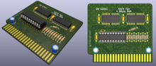
Hello everyone! My name is Zane, and this is my first post on the AppleFritter forum :). I'm posting to announce the coming availability of my 4 Mbyte Apple IIgs DRAM card, shown below:
Why did I make the card?Some time ago, I acquired three Apple IIgs systems (along with a bunch of Macintoshes) and have been restoring the machines on-and-off since. When I realized the necessity of RAM expansion for the IIgs (especially the earlier ROM systems), I figured I'd make my own RAM cards, keeping three and selling the rest. If there is continued demand, I can make more. I plan to offer the card for $30-35, fully assembled.
Engineering DetailsThe card provides 4 megabytes of DRAM. The model number is GW4201C... Some other in-progress designs of mine have other numerical designators, and this is the "C" revision of the card. The "A" revision had the logic associated with the RAM implemented in 7400 chips, and "B" lacked the little chin pointing toward the rear ports. Those revisions were abandoned before completion. I never manufactured or tried those ones out.
Two 16Mbit x4 DRAM ICs in (1990's) industry standard SOJ-24/SOIC-24 packaging implement the main DRAM storage. These are shown at the top of the card. I really wanted to use only a single 8-bit DRAM, rather than two 4-bit ones, but 32 Mbit DRAM is basically nonexistent (only even power of two sizes exist), and 64Mbit 5V DRAM is really hard to find. I wanted to avoid putting voltage regulators and level shifters and that kind of stuff on my board, so the largest easily-obtainable 5V DRAM chips were used.
A single GAL16V8-type device implements a bit of special logic required for proper operation of the DRAM ICs. This is the socketed DIP-20.
As has been written about in extent elsewhere, the 1Mbit DRAM spec is slightly less specific than the 4- and 16Mbit spec, and so the write-enable signal coming from the IIgs must be properly inactivated during refresh cycles. My GAL-based implementation of this gating circuit differs from other publicly-available designs in its functionality and implementation. At the beginning of each DRAM access cycle, be it a "normal" RAS-before-CAS cycle, or a CAS-before-RAS refresh cycle, a "write enable enable" (nWEE) signal is latched. Only during regular RAS-before-CAS cycles is the nWEE signal enabled. The GAL device then buffers the nWE signal coming from the IIgs, gating it according to the internally-generated nWEE. For ease of routing, two nWE outputs are produced, with one sent to each DRAM chip.
As well, compatibility with the 16 Mbit DRAM ICs requires multiplexing of the CROW0 and CROW1 signals coming from the IIgs onto a single address line of the IIgs. The GAL does this as well, sending CROW1 when nRAS is inactive, and CROW0 with nRAS active. Hold time of this address bit signal after nRAS becomes active is somewhat adjustable, up to 40 ns or so (the 16Mbit spec requires 10 or 15 ns, as I recall).
A great deal of attention has been paid to signal integrity. Most of the control lines coming from the Apple IIgs (e.g. RAS, CAS, etc.) are series-terminated, so no termination was necessary for these signals. The address bus, however, is designed to drive some 32 DRAM ICs, and so it is unterminated and has a relatively strong drive strength. Therefore termination is provided for the DRAM address signals coming onto the card. I plan to use at least 33 ohms, but likely more. The aim is to have the lowest drive strength and slew rate but without violating the minimum slew rate spec of the DRAM chips. The single multiplexed address signal coming from the GAL and going to the DRAM is also series-terminated, although the necessity of this is not clear. A ground grid design was used to minimize impedance discontinuities and avoid reference plane crossings. These measures, along with the small size of the card, ensure excellent signal integrity with only a 2-layer PCB.
What next?In a few weeks I will be receiving some prototype units which I will assemble and test. One I'm sure it works, if there is interest in purchasing the card, I will make them available for sale. Also in a week or two I will be announcing another product for Macintosh Plus. Some on the forum may be familiar with my earlier efforts at producing a Macintosh accelerator. Well that work is difficult and still ongoing, but I will be announcing a Macintosh Plus product a bit more novel and interesting than this RAM card.
Best Regards,Zane
I would also be interested in this board as a kit. $30-$35 for an assembled unit is a great deal.
I have surface-mount soldering equipment, so no issue with that.
Also have PROM burning as well. Let me know if you need help with assemblies.
Question: Why did you use discreet resistors instead of a resistor pak?
[quote=macnoyd]
I would also be interested in this board as a kit. $30-$35 for an assembled unit is a great deal.
I have surface-mount soldering equipment, so no issue with that.
Also have PROM burning as well. Let me know if you need help with assemblies.
Question: Why did you use discreet resistors instead of a resistor pak?
[/quote]
I may make it available as an unpopulated board or kit too, just let me see how many people want which one. I figured most people would want an assembled board.
The main reason for the discrete resistors is the ground routing of the card. The +5V power to run the GAL in the center of the board runs under the resistors on the bottom layer, as shown in this rear shot:
GW 4201C Rear
If I used resistor packs, then traces on the front layer would have to cross that gap created in the ground plane by the +5V trace. This is in general a no-no, since it would cause all of the return current on the ground plane from the signals driving the address bus to diverge fron the outgoing signal, creating more crosstalk and interference between the address bus signals and other signals in the area. With this design, the ground fill on the top layer of the board is kept solid, and the current traversing the resistor is allowed to return right below the resistor. So the resistors are used sort of like a jumper.
[/quote]
Congrats Zane on a well designed board. Although as a designer of many Apple II boards in the 70's and 80's I can tell you that such modern PCB layout considerations were not too important with the Apple II's lowly 1 or 2MHz clock frequencies. Bus termination and ground bounce certainly were; but trace equalization and even ground planes were rarely seen.
This reminds me of the ads from Monster Cable. They sold ridiculously expensive items such as shielded power cords and oxygen free litz wire audio cables (to reduce the skin effect - at AUDIO frequencies, no less!). A lot of hype and physics mumbo jumbo in their ads. Which is not to say that they were not great cables with gold plated connectors, etc. Just overkill for the intended use.
Bottom line is that it doesn't hurt to do things right. And you're certainly not charging more for that. Let me know when they're ready for sale.
i would be interrested in one (populated)
The first set of 10 boards have been in production since Monday morning and are likely to be done by the beginning of next week. Then after another week or so, I’ll receive the first boards and verify their functionality.
Now I have a question for those interested in purchasing the card as an unaasembled kit: Do you want the two surface-mount DRAM chips already soldered on the board, so that there is only through-hole soldering to be done? Or do you want to solder those two surface-mount RAM chips along with the surface-mount stuff? They’re pretty big as far as surface-mount goes, with 1.27mm pin spacing (half that of a DIP chip), so I don’t have much trouble soldering them, but I’ve invested a lot in my soldering equipment, and absent a better soldering setup, I could see it being a little difficult.
Hi Zane,
For me, a bare board and the chips (all parts) are fine. (completely unassembled)
Already have the equipment for it and I actually enjoy the assembly process.
If I could get them this way, I would start with 2 boards.
I’ve received the first boards and assembled one:
GW4201C Prototype
I will put units for sale through my ultrasonic cleaner to try and get rid of any flux residue on the board from soldering.
Well, the IIgs doesn’t crash, so that’s a start:
GW4201C Test Setup
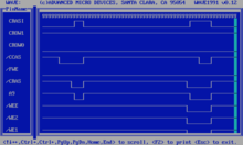
Using my trusty HP 54622D scope, I was able to capture some shots of the GAL’s functionality, multiplexing CROW1..0 onto A9 and also gating /WE during CAS-before-RAS refresh cycles.
PRINT_01.jpg
One thing I was worried about is the hold time of the single row address bit coming from the GAL. The GAL sends CROW1 on A9 as the row address when /RAS is high, and switches to CROW0 for the column address phase of the access when /RAS is low. The 60ns EDO/FPM DRAM spec requires that the row address be held for 10 nanoseconds after the falling edge of /RAS. However, the GAL I am using is specified to change its outputs in 15 ns or less. So the GAL may be a little too fast.
The solution was for the GAL to to buffer (invert) the /RAS signal and to feed it back into one of its inputs externally. This buffered signal is used to multiplex A9. An optional capacitor on the RAM board allows the delay to be increased a little further. I didn’t populate this and just tried with only the external feedback delay. The 54622D scope is a little slow (100 MHz, 200 MSa/s) to measure this hold time, so I switched to the slightly older but much faster HP 54542A scope, with all of 500 MHz and 2 GSa/s. Here is the result:
PRINT_00.png
The shot is in persistence mode, with a bunch of captures superimposed. On top are /RAS coming from the IIgs and RAS as inverted by the GAL. On the bottom, A9 is shown. I measured about 18 ns of hold time for A9 after /RAS falls with this GAL16V8D. Hmm, that’s okay but a little more hold time wouldn’t hurt in case I one day use a faster GAL. The column address just has to be presented within 100 ns or so. I will try changing the GAL programming a little, running the RAS signal through the GAL internally a few more times to delay it further.
That’s all for tonight. Tomorrow I’ll try a RAM test program.
Success! Using the GMT memory test (https://gglabs.us/node/2050) I was able to verify that the RAM card works as intended:
51641423-927D-4A13-BAD7-E7FEDBF06323.jpeg
Information on how to buy is forthcoming but there is a little supply issue. I have 10 PCBs which I can assemble now or sell as kits, but they are not gold-plated. They've got the standard silvery tin-lead "HASL" finish (despite the golden appearence of the pads on the board in the picture in my last post... they are indeed not gold plated)
Gold PCBs are forthcoming with a slightly modified visual design. A rendering of the new board revision is shown below. It's supposed to look like a caricature of the original Apple-designed RAM expansion card:
4201A
However there is an issue! Right now is the Chinese Lunar New Year, a 3-4 week festival celebrated in China which has just begun. No PCBs can be ordered from any of the Chinese fabrication companies until mid-February, so the gold-plated boards will not be available for another month at least. So the silver-colored tin-lead plated boards will be offered at a reduced price of $30 each.
I anticipate it will take another week for me to source the requisite parts, and then I will contact everyone who's expressed interest and ask them about their preferences. Ordering options will be:
slightly-older-design tin-lead plated boards OR newer-design gold-plated boards
unassembled OR just the surface-mount chips OR fully assembled